Memory module with a defective memory chip having defective blocks disabled by non-multiplexed address lines to the defective chip

a memory module and chip technology, applied in the field of memory module manufacturing, can solve the problems of noisy test environment, wafer-sort test may not catch all defects, and manufacturing defects to be somewhat common

Active Publication Date: 2007-10-02
KINGSTON DIGITAL CO LTD
View PDF16 Cites 23 Cited by
  • Summary
  • Abstract
  • Description
  • Claims
  • Application Information

AI Technical Summary

Problems solved by technology

The large number of memory cells, small size of individual memory cells, and overall large area of the DRAM die cause manufacturing defects to be somewhat common.
DRAM chips are tested on a wafer before being separated and packaged, but this wafer-sort test may not catch all defects.
A probe card is used to make contact with individual die on the wafer, causing a very noisy test environment.
Thus test speeds are limited at wafer sort, preventing more exhaustive testing that could catch more defects.
Thus some packaged DRAM chips are going to contain defects.
However, discarding packaged DRAM chips is somewhat wasteful, since often only a single defect is present.
For example, a defect may cause only 1 of the half-billion memory cells to fail.
Nearly half a billion memory cells operate properly on a DRAM chip having a single defect, yet this chip is typically discarded.
Repair often causes the full size of memory to be available when repair is successful.
Rather than repairing chips, some chip manufacturers may downgrade DRAM chips to lower capacities.

Method used


Image

  • Memory module with a defective memory chip having defective blocks disabled by non-multiplexed address lines to the defective chip
  • Memory module with a defective memory chip having defective blocks disabled by non-multiplexed address lines to the defective chip
  • Memory module with a defective memory chip having defective blocks disabled by non-multiplexed address lines to the defective chip

Examples


Embodiment Construction

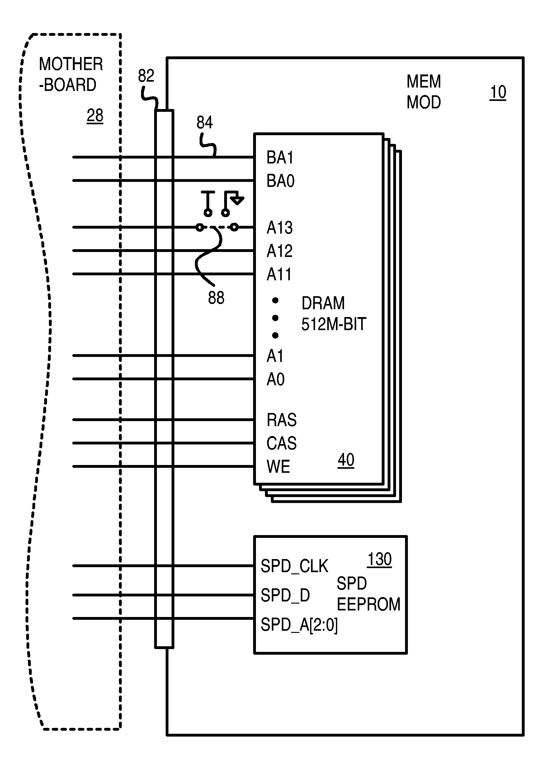
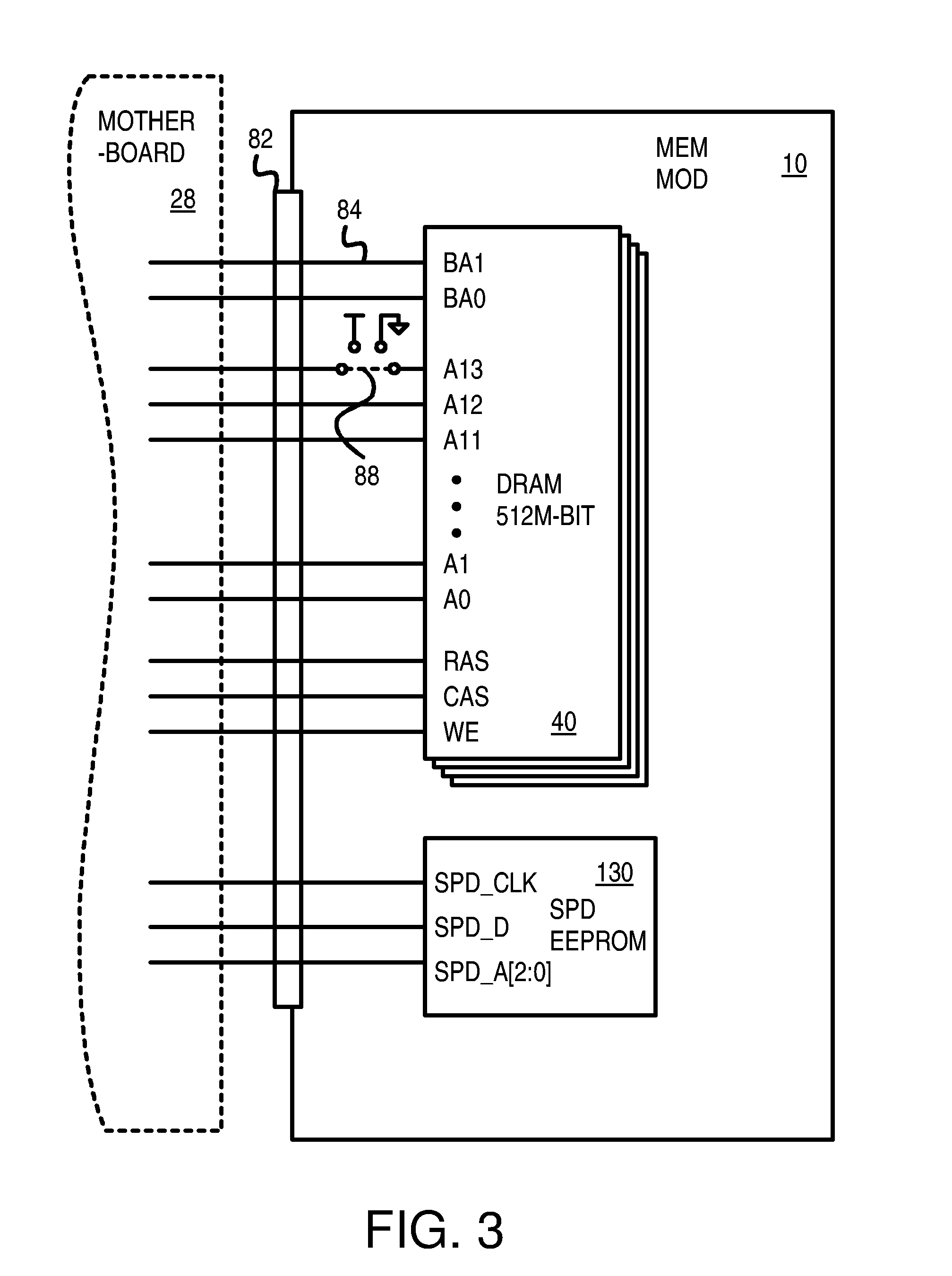
[0025]The present invention relates to an improvement in memory module manufacturing. The following description is presented to enable one of ordinary skill in the art to make and use the invention as provided in the context of a particular application and its requirements. Various modifications to the preferred embodiment will be apparent to those with skill in the art, and the general principles defined herein may be applied to other embodiments. Therefore, the present invention is not intended to be limited to the particular embodiments shown and described, but is to be accorded the widest scope consistent with the principles and novel features herein disclosed.

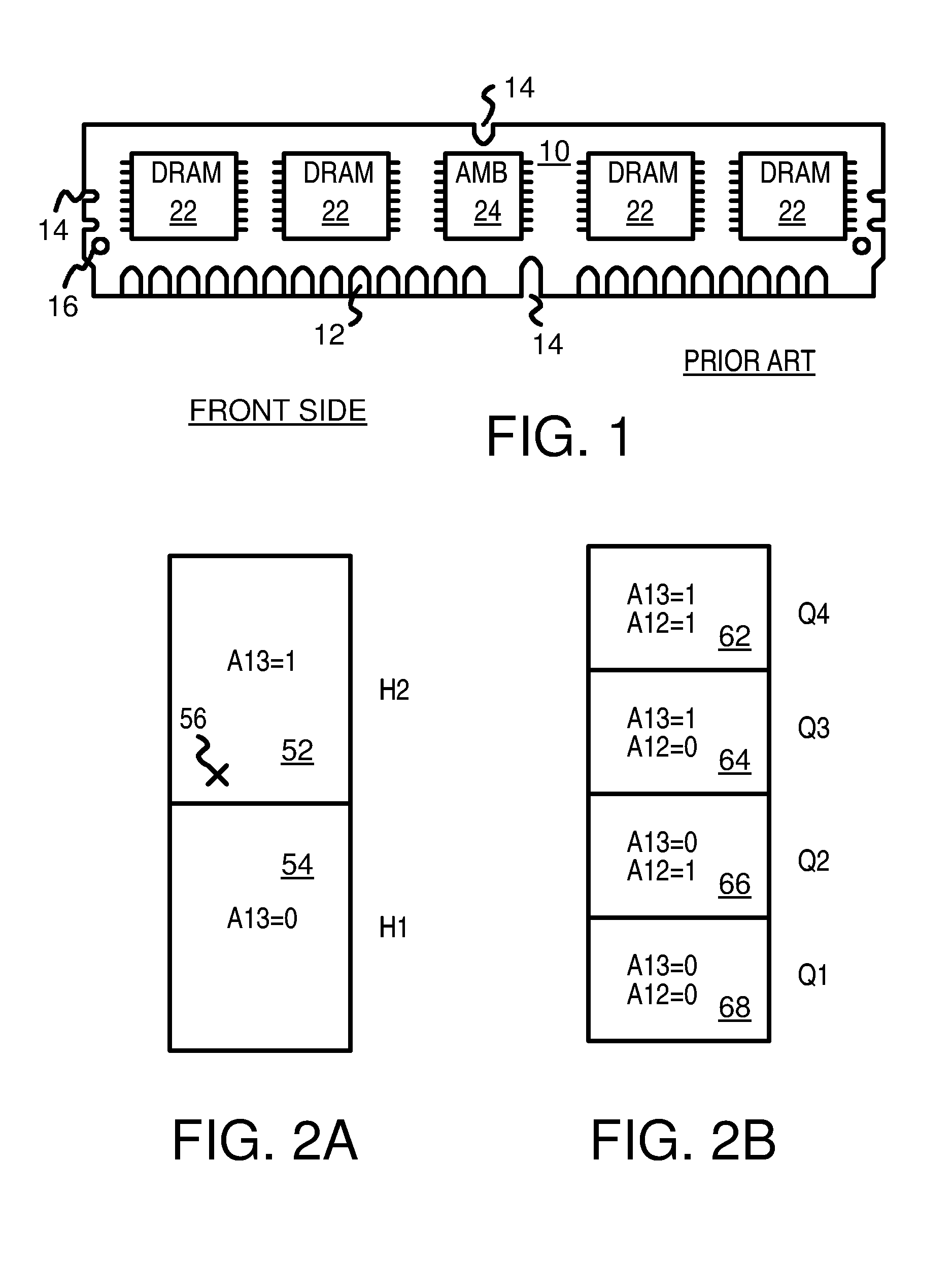
[0026]FIGS. 2A-B show a defect on a downgradable DRAM chip. In FIG. 2A, DRAM chip has an upper address bit A13 that divides the memory into two halves H1, H2. The halves H1, H2 may be logical halves rather than separate physical arrays on the DRAM die. When address A13=1, half H2 is selected, while when A13=0, half H1 is s...


PUM


Abstract

A downgraded memory module has downgraded DRAM chips soldered to its substrate. The downgraded DRAM chips have a defective memory cell in a logical quadrant of the memory. A physical MSB is a row address present on a non-downgraded DRAM of size S but not used on a downgraded DRAM size S / 2. The physical MSB and a second address pin are non-multiplexed address pins that do not carry column addresses. The physical MSB and the second address pin logically divided the DRAM into quadrants. Two good quadrants without defects are selected, and jumpers on the memory module drive the physical MSB and the second address pin with signals that select only these two quadrants and disable access to quadrants containing defects. DRAM chips can be marked or sorted into bins for combinations of good quadrants. Downgraded memory modules have all DRAM chips from the same bin that share jumper settings.

Description

FIELD OF THE INVENTION[0001]This invention relates to memory-module manufacturing, and more particularly to testing and using downgraded memory chips.BACKGROUND OF THE INVENTION[0002]Memory modules are widely used in a variety of electronic systems, especially Personal Computers (PC's). Memory modules are built to meet specifications set by industry standards, thus ensuring a wide potential market. High-volume production and competition have driven module costs down dramatically, benefiting the PC buyer.[0003]Memory modules are made in many different sizes and capacities, such as older 30-pin and 72-pin single-inline memory modules (SIMMs) and newer 168-pin, 184-pin, and 240-pin dual inline memory modules (DIMMs). The “pins” were originally pins extending from the module's edge, but now most modules are leadless, having metal contact pads or leads. The modules are small in size, being about 3-5 inches long and about an inch to an inch and a half in height.[0004]The modules contain a...

Claims


Application Information

Patent Timeline
Patent Type & Authority Patents(United States)
IPC IPC(8): G11C29/00
CPCG11C5/04G11C29/883G11C29/88G11C2029/4402
Inventor CO, RAMON S.CHEN, MIKESUN, DAVID
Owner KINGSTON DIGITAL CO LTD
Why Eureka
Try Eureka