Semiconductor package

a technology of semiconductors and components, applied in the direction of printed circuit aspects, sustainable manufacturing/processing, final product manufacturing, etc., can solve the problems of poor solder connection, frame packages are not capable of providing chip solutions, and traditional lead frame packages have been gradually obsolete for some high-efficiency integrated circuit products. achieve the effect of increasing the height of the solder and increasing the strength of the solder connection

Active Publication Date: 2007-10-09
ADVANCED SEMICON ENG INC
View PDF8 Cites 53 Cited by
  • Summary
  • Abstract
  • Description
  • Claims
  • Application Information

AI Technical Summary

Benefits of technology

[0009]It is an object of the present invention to provide a semiconductor package in which the solder fillet height can be effectively increased without increasing the overall thickness of the package itself, thereby increasing the strength of the solder connection and overcoming or at least improving the above-mentioned problem in the prior art.
[0012]The L-shaped leads (or J-shaped leads) exposed out of the bottom of the semiconductor package are respectively bonded to a plurality of corresponding pads on a printed circuit board by solder when the above semiconductor package is attached on a substrate, e.g. a printed circuit board, by surface mount technology (SMT). Compared to the conventional leadless package, the outer lead portion of the L-shaped lead (or J-shaped lead) according to the present invention can effectively increase the solder fillet height while the overall thickness of the semiconductor package according to the present invention is kept close to that of the above-mentioned conventional leadless package. Although the outer lead portion of the L-shaped lead (or J-shaped lead) according to the present invention may slightly increase the overall volume of the semiconductor package, the footprint area of the outer lead portion will not cause great effects upon the layout of the printed circuit board. Further, the semiconductor package according to the present invention can be obtained by lengthening the leads of the conventional lead frame and then punching and cutting the lengthened leads so as to form the L-shaped leads (or J-shaped leads). Therefore, the semiconductor package according to the present invention can utilize existing BOM (bill of materials) such that it has high price competitiveness.

Problems solved by technology

However, as integrated circuit products are becoming faster in speed and smaller in volume, the traditional lead frame packages have been gradually obsolete for some high-efficiency integrated circuit products.
The traditional lead frame packages are not capable of providing a solution for chip scale and low profile packages due to their long inner leads and outer leads.
In the conventional surface mount technology (SMT) for mounting the leadless package 10 to the substrate 16, there exists a problem that the area of the inner leads 11a exposed out of the bottom of the leadless package 10 is too small and therefore causes poor solder connection and poor reliability.

Method used


Image

  • Semiconductor package
  • Semiconductor package
  • Semiconductor package

Examples


Embodiment Construction

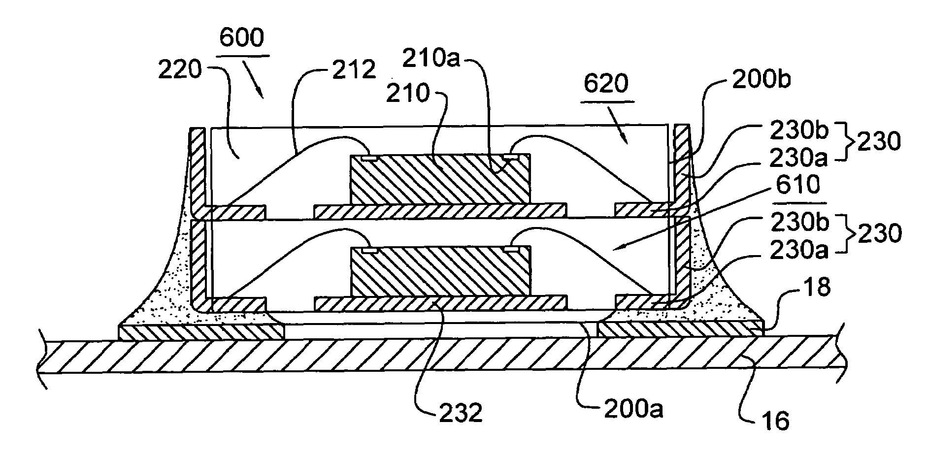
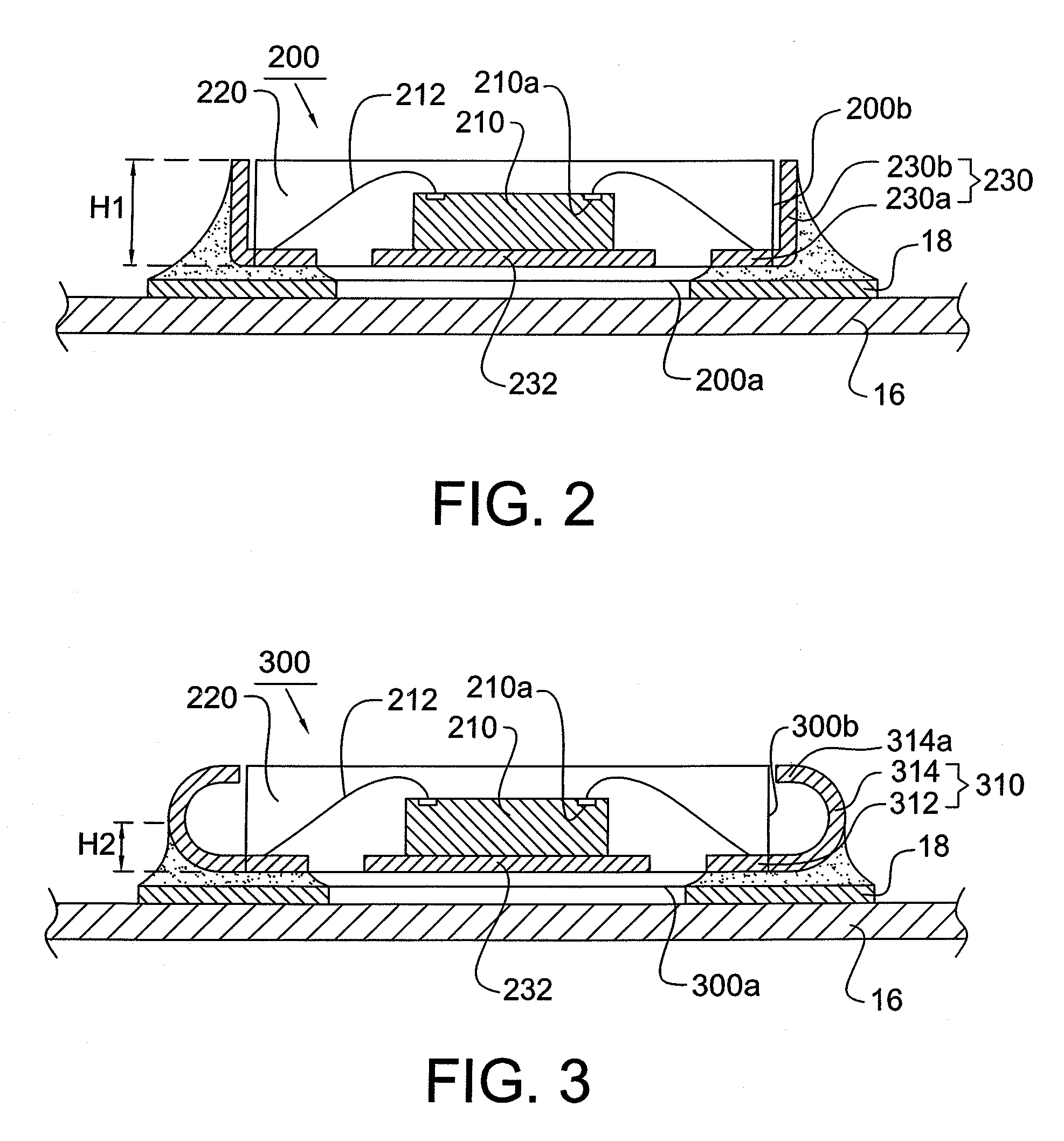
[0024]FIG. 2 shows a semiconductor package 200 according to one embodiment of the present invention. The semiconductor package 200 comprises a semiconductor chip 210 attached to a die pad 232 by a conductive or nonconductive adhesive, e.g. epoxy adhesive (not shown). The semiconductor chip 210 has a plurality of bonding pads 210a disposed on its active surface, wherein the bonding pads 210a are electrically connected to a plurality of L-shaped leads 230 through a plurality of bonding wires 212. The L-shaped leads 230 are arranged at the periphery of the semiconductor chip 210. Each L-shaped lead 230 has an inner lead portion 230a exposed out of the lower surface 200a of the semiconductor package and an outer lead portion 230b extending from the inner lead portion 230a and exposed out of the semiconductor package. The outer lead portion 230b is formed substantially parallel to and adjacent to the side surface 200b of the semiconductor package. A package body 220 is formed over the se...


PUM


Abstract

A semiconductor package mainly includes a semiconductor chip and a plurality of L-shaped leads arranged at the periphery of the semiconductor chip. Each of the L-shaped leads has an inner lead portion exposed out of the lower surface of the semiconductor package and an outer lead portion formed substantially parallel to and adjacent to one of the side surfaces of the semiconductor package. The semiconductor chip has a plurality of bonding pads electrically coupled to the inner lead portions of the L-shaped leads. The semiconductor package is provided with a package body formed over the semiconductor chip and the inner lead portions of the L-shaped leads.

Description

BACKGROUND OF THE INVENTION[0001]1. Field of the Invention[0002]This invention generally relates to a lead frame package.[0003]2. Description of the Related Art[0004]Lead frame packages have been widely used for a long time in the IC packaging field due to their low manufacturing cost and high reliability. However, as integrated circuit products are becoming faster in speed and smaller in volume, the traditional lead frame packages have been gradually obsolete for some high-efficiency integrated circuit products. Accordingly, ball grid array (BGA) packages and chip scale packages (CSP) have become popular packaging choices. The ball grid array (BGA) packages have been widely used in IC chips having high I / O count and requiring good electrical and thermal efficiencies, e.g. CPU chips and graphic chips. In addition, the chip scale packages (CSP) have been widely used in mobile products; the footprint size, package profile and package weight are major concerns for the chip scale packag...

Claims


Application Information

Patent Timeline
Patent Type & Authority Patents(United States)
IPC IPC(8): H01L23/02H01L23/31H01L23/495H01L25/10H05K3/34
CPCH01L23/3107H01L23/49555H01L25/105H05K3/3426H01L2224/48091H01L2224/48247H01L2225/1029H05K2201/10689H05K2201/10772H01L24/48H01L2924/00014H01L2924/14H01L2924/181Y02P70/50H01L2924/00H01L2924/00012H01L2224/45099H01L2224/45015H01L2924/207
Inventor LIU, SHENG TSUNG
Owner ADVANCED SEMICON ENG INC
Why Eureka
Try Eureka