Three-dimensional non-volatile SRAM incorporating thin-film device layer

a technology of sram and thin film, applied in the direction of static storage, digital storage, instruments, etc., can solve the problems of limiting the suitability of certain applications, the number of program/erase cycles, and other non-volatile technologies, and achieve the effect of low-cost memory devices

Active Publication Date: 2007-10-09
SANDISK TECH LLC
View PDF11 Cites 55 Cited by
  • Summary
  • Abstract
  • Description
  • Claims
  • Application Information

AI Technical Summary

Benefits of technology

[0008]A shadow RAM or “non-volatile SRAM” memory cell may be implemented in a much smaller area by building the cell upward rather than outward. For example, by stacking thin film non-volatile storage devices on top of an SRAM cell largely formed on the semiconductor substrate, a smaller cell can be provided and result in a lower cost memory device.

Problems solved by technology

The design and configuration of semiconductor memory devices frequently must make trade-offs in area, performance, power dissipation, environmental requirements, and volatility.
Some memory technologies are high performance, but are volatile (e.g., lose data when powered off), while other technologies are non-volatile but lower in performance.
Some non-volatile memory technologies also have limitations on the number of program / erase cycles that may be performed, which limits their suitability for certain applications.
This adds cost, risks such batteries being discharged too quickly when needed, and may also negatively impact overall reliability.

Method used


Image

  • Three-dimensional non-volatile SRAM incorporating thin-film device layer
  • Three-dimensional non-volatile SRAM incorporating thin-film device layer
  • Three-dimensional non-volatile SRAM incorporating thin-film device layer

Examples


Embodiment Construction

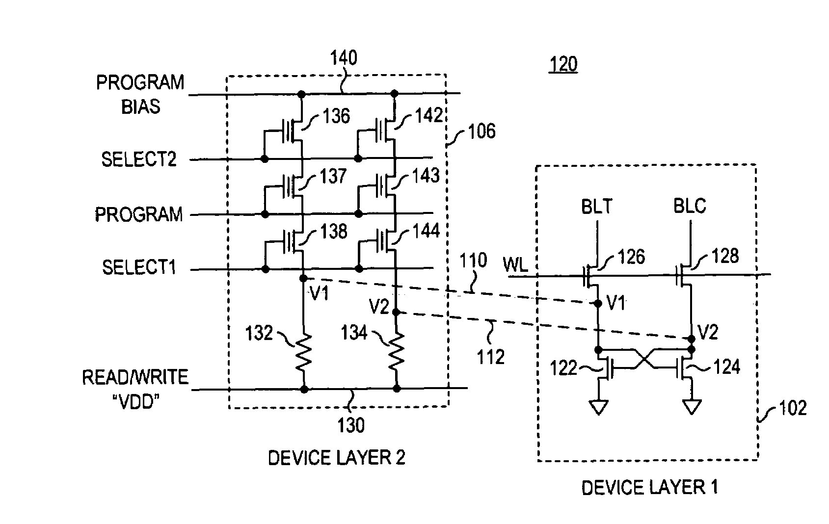
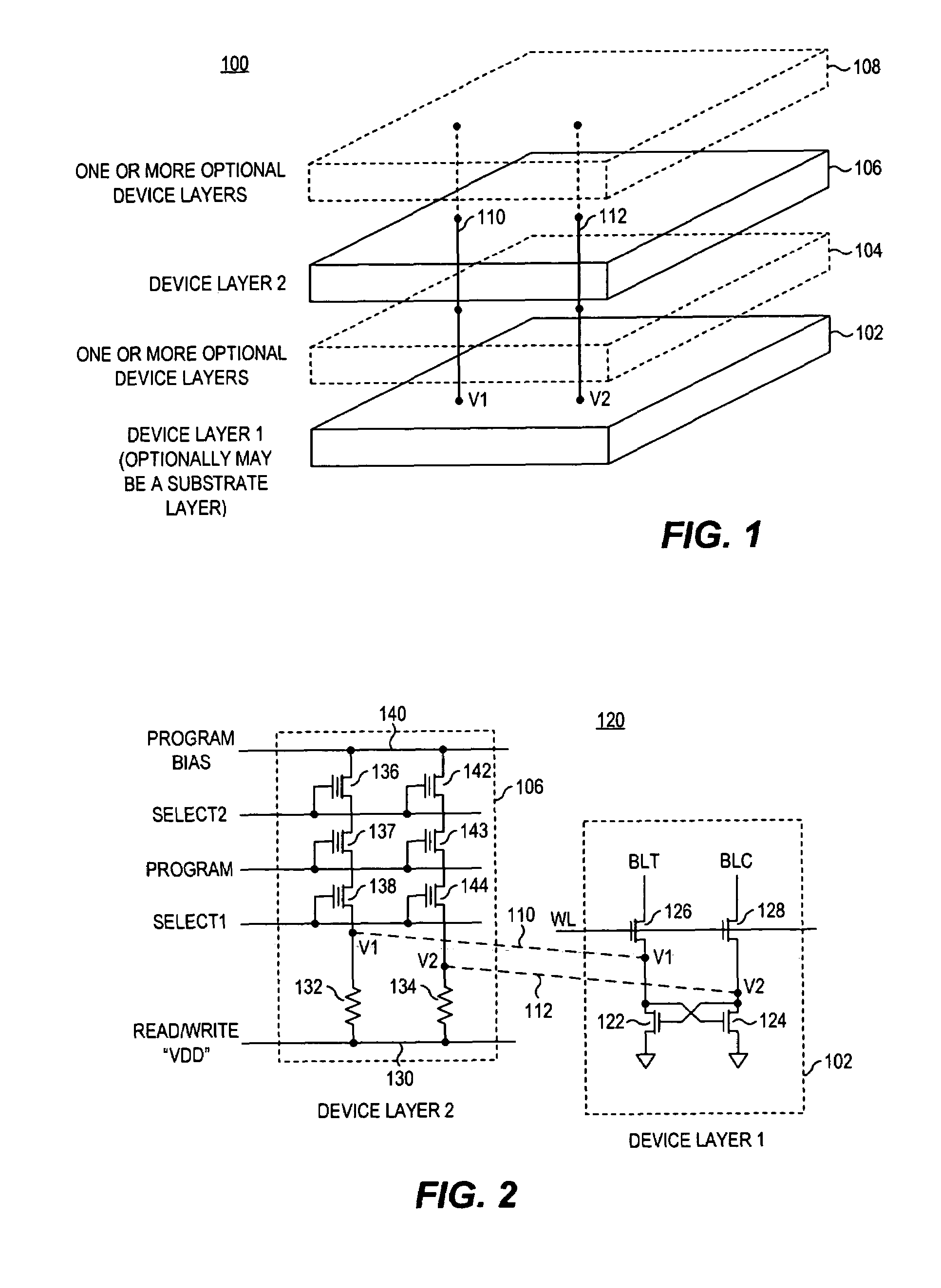
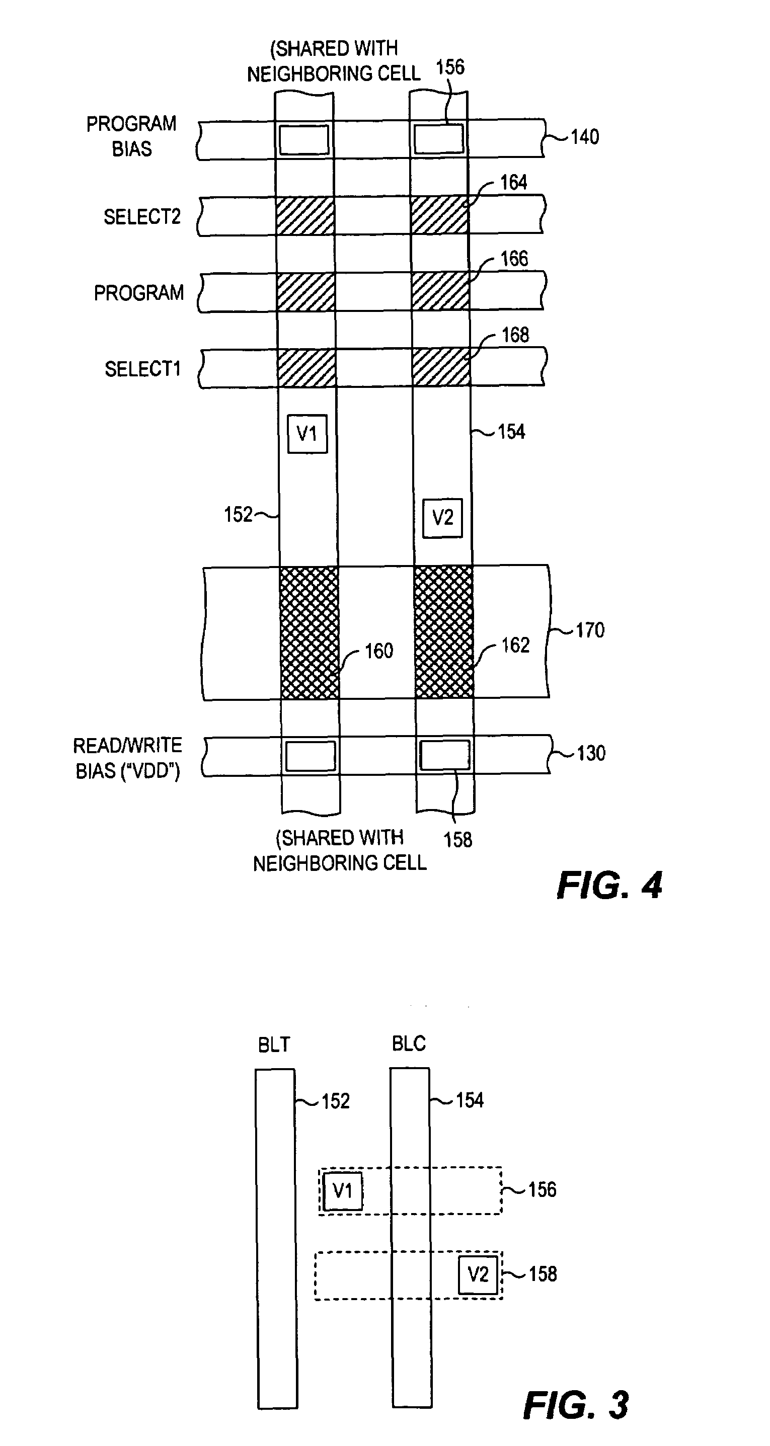
[0026]Referring now to FIG. 1, a structural representation is shown of a non-volatile memory cell 100 which includes a device layer 102 and at least a second device layer 106. One or more optional layers 104 may be disposed between device layer 102 and device layer 106, and one or more optional-device layers 108 may be disposed above device layer 106. Such a memory cell is suitable for fabrication in a monolithic integrated circuit. One of the device layers, such as device layer 102, may be a substrate layer, such as a semiconductor substrate device layer (e.g., one or more layers and features useful for forming a traditional silicon gate transistor upon a semiconductor substrate), although such is not required. Such device layers may also be formed of a thin film semiconductor layer, within which may be formed transistors, resistors, or other useful components. Informally, such a layer may be referred to as a TFT layer (i.e., “thin film transistor” layer) even though such a layer m...


PUM


Abstract

A shadow RAM or “non-volatile SRAM” memory cell is implemented in a much smaller area by building the cell upward rather than outward. By stacking non-volatile storage devices above or below an SRAM cell, a smaller cell can be provided and result in a lower cost memory device. In certain embodiments, such a memory cell includes a pair of cross-coupled devices disposed on a first device layer and defining a pair of internal cross-coupled nodes, and a pair of non-volatile storage devices disposed on a second device layer above or below the pair of cross-coupled devices and coupled to the cross-coupled nodes.

Description

BACKGROUND[0001]1. Field of the Invention[0002]The present invention relates to read / write semiconductor memory devices, and particularly to such devices including both volatile and non-volatile data storage within each memory cell and which are sometimes referred to as shadow RAMs.[0003]2. Description of the Related Art[0004]The design and configuration of semiconductor memory devices frequently must make trade-offs in area, performance, power dissipation, environmental requirements, and volatility. Some memory technologies are high performance, but are volatile (e.g., lose data when powered off), while other technologies are non-volatile but lower in performance. Some non-volatile memory technologies also have limitations on the number of program / erase cycles that may be performed, which limits their suitability for certain applications.[0005]To achieve a high performance non-volatile memory, batteries have sometimes been incorporated into the packaging of otherwise volatile semic...

Claims


Application Information

Patent Timeline
Patent Type & Authority Patents(United States)
IPC IPC(8): G11C14/00
CPCG11C14/0063G11C14/00
Inventor SCHEUERLEIN, ROY E.
Owner SANDISK TECH LLC
Why Eureka
Try Eureka