BLEQ driving circuit in semiconductor memory device

a driving circuit and semiconductor technology, applied in the direction of information storage, static storage, digital storage, etc., can solve the problems of reducing the driving performance of the boosted voltage vpp, affecting the performance of the memory cell, and consuming low power, so as to prevent the deterioration of trp performance and current waste

Active Publication Date: 2007-10-09
SK HYNIX INC
View PDF11 Cites 10 Cited by
  • Summary
  • Abstract
  • Description
  • Claims
  • Application Information

AI Technical Summary

Benefits of technology

[0013]It is, therefore, an object of the present invention to provide a memory device capable of preventing the deterioration of tRP performance and current waste required in generating a boosted voltage VPP which is used to drive its bit line equalization signal driving circuit.

Problems solved by technology

As a result, the memory cell has a very small size and consumes low power.
Moreover, since switches existing at several places in the memory device having cell transistors are mostly formed with MOS transistors, there exists the voltage loss due to gate voltage drop (Vt) of the MOS transistors.
However, when using this scheme, the driving performance of the boosted voltage VPP may be substantially deteriorated in a range of an operational voltage being lower than 2.0V.
In particular, this phenomenon becomes more serious in the low power environment.
As a result, the driving performance of the boosted voltage is substantially deteriorated.
Furthermore, word line enablement performed by the boosted voltage VPP is also delayed or there may occur a problem in a refresh operation due to the voltage level down.
Also, current consumption increases by driving the boosted voltage generator so as to elevate the dropped voltage level of the boosted voltage.
However, if applying the conventional bit line precharging scheme using the supply voltage VDD to the low power memory device, there occurs speed delay by a relatively boosted back bias and a lowered supply voltage, resulting in deteriorating a time constant tRP relating to a precharge time.
That is, in case of using the supply voltage VDD as the BLEQ signal, since a time required in adjusting voltage level of relating circuits to a precharge voltage VBLP becomes longer, it is difficult to set the relating circuits with the precharge voltage VBLP before a next active time tRP.
As a result, the possibility of a precharge operation to be failed becomes higher.

Method used


Image

  • BLEQ driving circuit in semiconductor memory device
  • BLEQ driving circuit in semiconductor memory device
  • BLEQ driving circuit in semiconductor memory device

Examples


Embodiment Construction

[0030]Hereinafter, with reference to the drawings, some of the preferred embodiments of the present invention will be explained in detail.

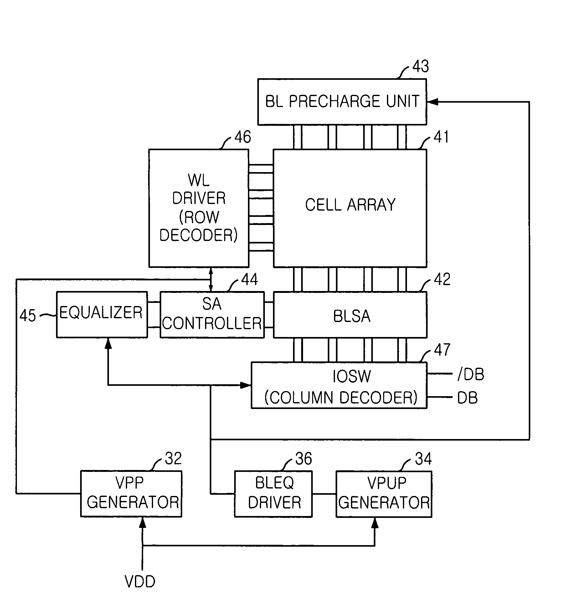
[0031]FIG. 3 shows a block diagram of a memory device in accordance with a first embodiment of the present invention.

[0032]The memory device described in FIG. 3 includes a core area, a first boosted voltage (VPP) generator 32, a second boosted voltage (VPUP) generator 34 and an equalization signal (BLEQ) driver 36.

[0033]Herein, the core area includes a cell array 41, a bit line (BL) precharge unit 43, a bit line sense amplifier (BLSA) 42, a word line (WL) driver 46, a sense amplifier (SA) controller 44, an equalizer 45 and an input / output switch (IOSW) 47.

[0034]The cell array 41 consists of a plurality of memory cells in which data are stored and the bit line (BL) precharge unit 43 adjusts a pair of bit lines with a precharge voltage. The bit line sense amplifier (BLSA) 42 amplifies voltage difference of the bit lines induced by a storage value of...


PUM


Abstract

A bit line equalization signal (BLEQ) driving circuit for generating an equalization signal used to perform a precharge operation in a semiconductor memory device includes a second boosted voltage generator for producing a second boosted voltage by pumping a supply voltage, a BLEQ driver for generating the equalization signal by using the second boosted voltage in response to an equalization command and providing the equalization signal to a precharge unit, an equalizer and an I / O switch module. By using the second boosted voltage VPUP, which is lower than a first boosted voltage and higher than the supply voltage, as the equalization signal to be provided to gates of transistors for precharging a low power device to a precharge voltage level, it is possible to save current that a voltage pump consumes and satisfy a constant tRP.

Description

FIELD OF THE INVENTION[0001]The present invention relates to a bit-line equalization signal (BLEQ) driving circuit used in a semiconductor memory device; particularly to a BLEQ driving circuit usable in the low voltage (VDD) environment and a semiconductor memory device employing the driving circuit.BACKGROUND OF THE INVENTION[0002]It becomes a trend to design a semiconductor memory device having high capacity and high operational speed. Furthermore, it is noticed that a memory device is designed to operate at low voltage or low power to acquire reliable performance at the low power environment. In particular, it is a trend to design a memory device employed in a portable system such as a mobile phone, a notebook computer, etc. to consume the minimum power if possible.[0003]One of the efforts is a technology of reducing current consumption at a core area of a memory device to the minimum. The core area including memory cells, bit lines and word lines is designed according to an extr...

Claims


Application Information

Patent Timeline
Patent Type & Authority Patents(United States)
IPC IPC(8): G11C7/12G11C7/00G11C11/4094
CPCG11C11/4094G11C5/145G11C7/12G11C11/4074G11C2207/2227
Inventor KIM, KYOUNG-NAMLEE, KANG-SEOL
Owner SK HYNIX INC
Why Eureka
Try Eureka