Method for forming a hard bias structure in a magnetoresistive sensor

a magnetoresistive sensor and hard bias technology, applied in nanoinformatics, instruments, manufacturing tools, etc., can solve the problems of difficult to obtain the free layer and the appropriate alignment of the hard bias layer using conventional processing methods

Inactive Publication Date: 2007-10-23
WESTERN DIGITAL TECH INC
View PDF11 Cites 161 Cited by
  • Summary
  • Abstract
  • Description
  • Claims
  • Application Information

AI Technical Summary

Benefits of technology

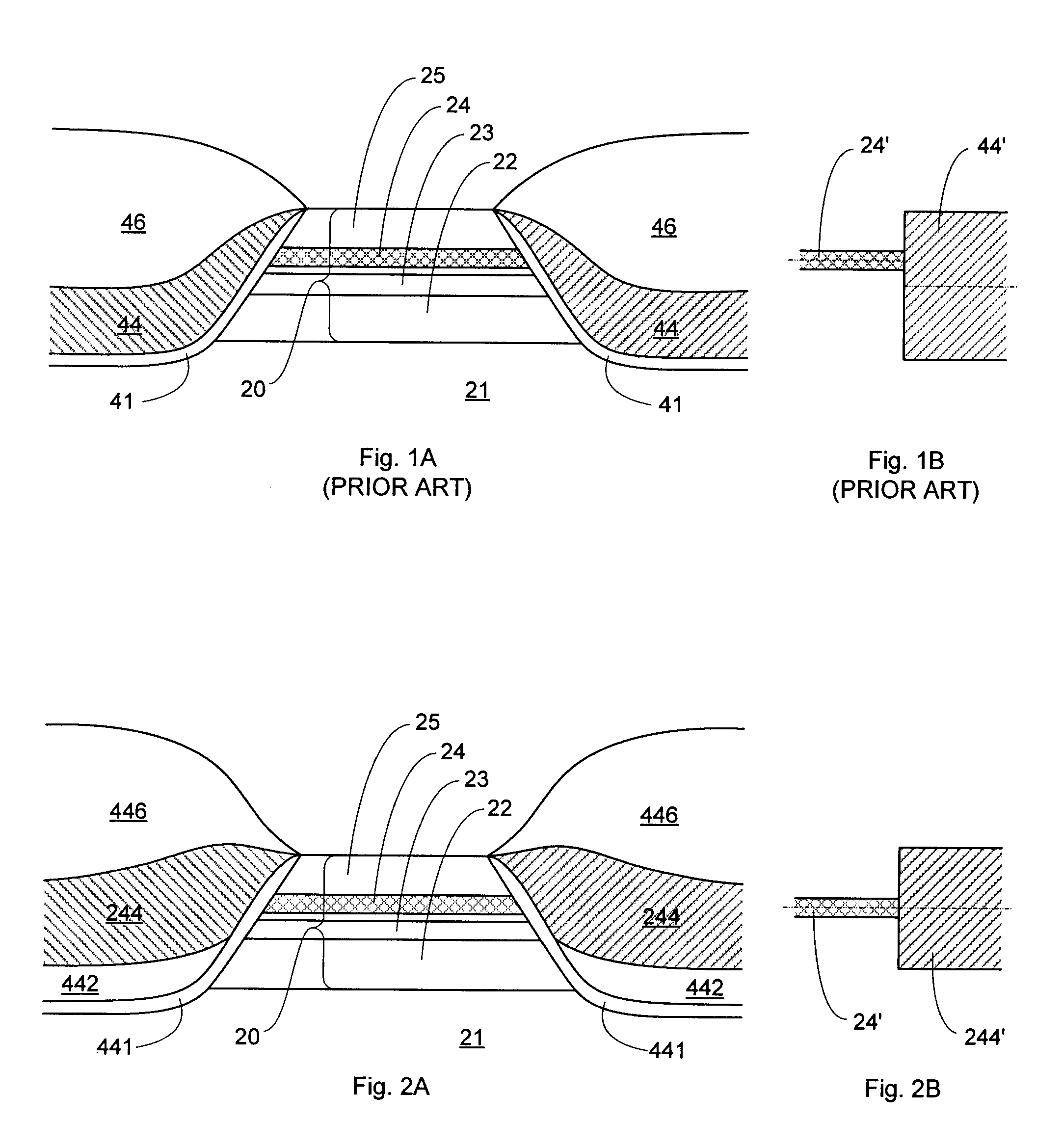
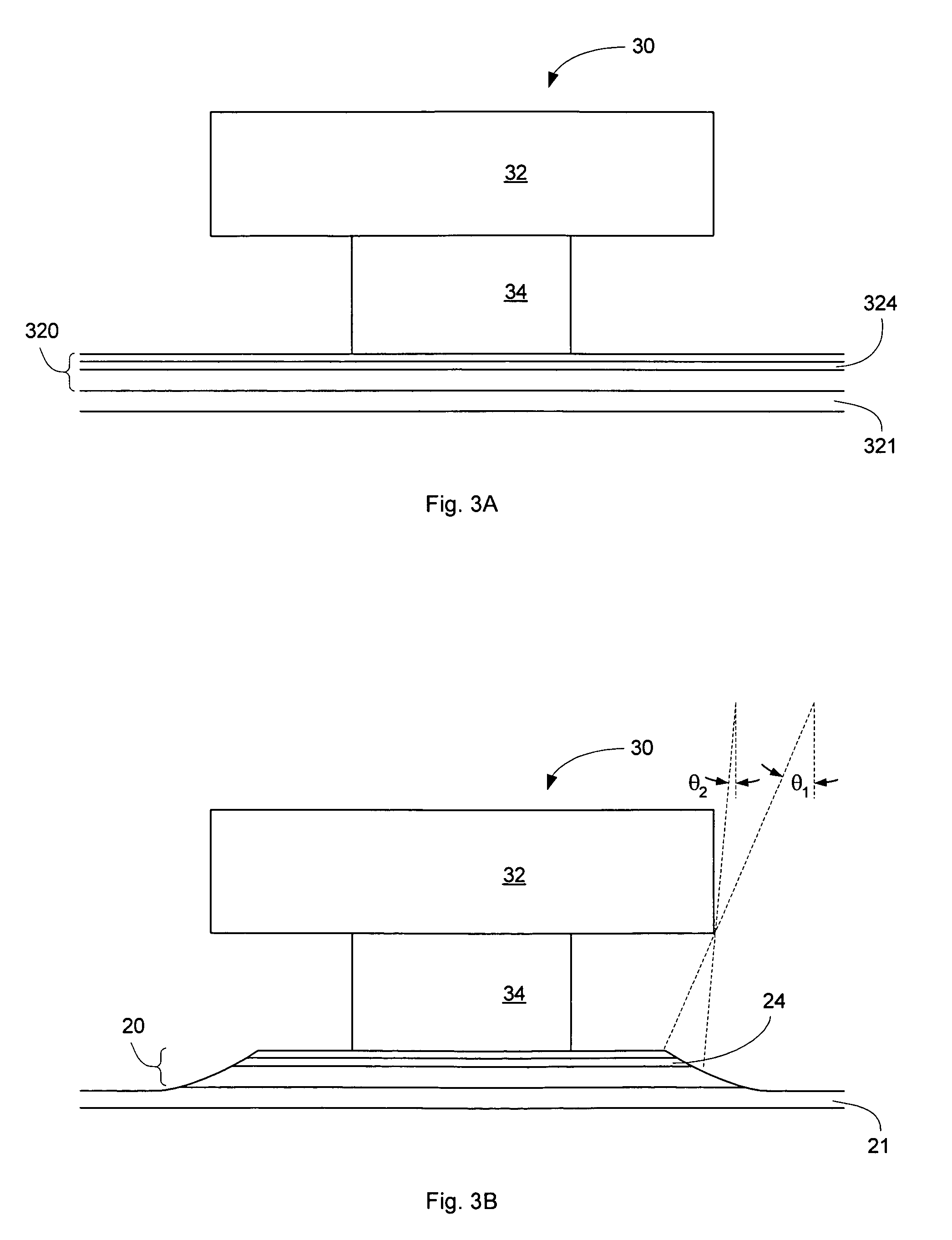
[0008]In one aspect the invention can be considered as a method for forming a hard bias structure in a magnetoresistive sensor, by: providing a substrate including a gap layer; forming magnetoresistive sensor structure over the substrate, the magnetoresistive sensor structure comprising at least a soft magnetic bias layer, a spacer layer over the soft magnetic bias layer, and a magnetoresistive layer over the spacer layer; forming a bilayer mask over the magnetoresistive sensor structure to define a central region of the magnetoresistive sensor, the mask having a narrower lower layer and a broader upper layer; ion milling the masked magnetoresistive structure to remove portions of the magnetoresistive sensor structure not shielded by the mask, to form a central region of the magnetoresistive sensor having sloped sides; forming a first underlayer onto the sloped sides of the central region and onto the exposed substrate by depositing a first underlayer material at a relatively high deposition angle (i.e. a first lower deposition angle); forming a second underlayer on a portion of the first underlayer by depositing second underlayer material at a relatively low deposition angle; and forming a hard bias layer on the second underlayer by depositing a hard bias material at a relatively low deposition angle (i.e. a second lower deposition angle).
[0009]In another aspect the invention can be considered as a method for making a magnetoresistive sensor, by: providing a substrate including a gap layer; forming a magnetoresistive sensor structure over the substrate, the magnetoresistive sensor structure comprising at least a soft magnetic bias layer, a spacer layer over the soft magnetic bias layer, and a magnetoresistive layer over the spacer layer; forming a bilayer mask over the magnetoresistive sensor structure to define a central region of the magnetoresistive sensor, the mask having a narrower lower layer and a broader upper layer; ion milling the masked magnetoresistive structure to remove portions of the magnetoresistive sensor structure not shielded by the mask, to form a central region of the magnetoresistive sensor having sloped sides; forming a first underlayer onto the sloped sides of the central region and onto the exposed substrate by depositing underlayer material at a relatively high deposition angle; forming a second underlayer on a portion of the first underlayer by depositing underlayer material at a relatively low deposition angle; forming a hard bias layer on the second underlayer by depositing hard bias material at a relatively low deposition angle; and forming leads over the hard bias layer.
[0010]In another aspect the invention can be considered as a magnetoresistive sensor, including: a central region including a free layer and having sloped sides, formed on a substrate including a gap layer; an underlayer covering the sloped sides and portions of the substrate laterally adjacent the central region, the underlayer having a thickness over the sloped sides in a range from about 20 Å to about 80 Å, more usually in a range from about 20 Å to about 70 Å, such as about 20 Å or about 30 Å, and having a thickness over the laterally adjacent substrate portions in a range from about 60 Å to about 250 Å, such as about 130 Å; and a hard bias layer over the underlayer.

Problems solved by technology

The thickness of the hard bias layer is much less than that of the spin valve structure, and appropriate alignment of the hard bias layer and the free layer is difficult to obtain using conventional processing methods.

Method used


Image

  • Method for forming a hard bias structure in a magnetoresistive sensor
  • Method for forming a hard bias structure in a magnetoresistive sensor
  • Method for forming a hard bias structure in a magnetoresistive sensor

Examples


example 1

[0048]In this example, the design height FL of the midplane of the free layer over the top surface of the gap is 200 Ångstroms, and the design depth T of the overmill is 20 Ångstroms. The required design thickness of the second Cr deposition (CRII, Ångstroms) for six selected hard bias thicknesses (HS, Ångstroms) and corresponding MRTs is shown in the following Table A:

[0049]

TABLE AMRTHSCRII2.530517.52250451.518776.51.2515791.511281060.7596122

example 2

[0050]In this example, the design height FL of the midplane of the free layer over the top surface of the gap is 300 Ångstroms, and the design depth T of the overmill is 10 Ångstroms. The required design thickness of the second Cr deposition (CRII, Ångstroms) for six selected hard bias thicknesses (HS, Ångstroms) and corresponding MRTs is shown in the following Table B:

[0051]

TABLE BMRTHSCRII3370752.5305107.522501351.5187166.51.25157181.51128196


PUM

PropertyMeasurementUnit
deposition angleaaaaaaaaaa

Abstract

A method for forming a hard bias structure in a magnetoresistive sensor is disclosed. A magnetoresistive sensor having a soft magnetic bias layer, spacer layer, and a magnetoresistive layer, is formed over a substrate having a gap layer. A mask is formed over a portion of the magnetoresistive sensor structure to define a central region. The masked structure is ion milled to remove portions not shielded by the mask, to form the central region with sloped sides, and to expose a region of the gap layer laterally adjacent the sloped sides. A first underlayer is deposited onto at least the sloped sides at a high deposition angle. A second underlayer is deposited to at least partially overlap the first underlayer, and at a first lower deposition angle. A hard bias layer is deposited over at least a portion of the second underlayer, and at a second lower deposition angle.

Description

BACKGROUND[0001]This invention relates to magnetic data read heads and, particularly, to a thin film magnetic read head having a magnetoresistive read transducer.[0002]A magnetic data storage system includes, generally, a storage medium, such as a tape or desk in which the data are stored in the form of small magnetized areas; a write element, which writes data to the storage medium by magnetizing the small data bits in the medium; and a read element, which senses the recorded magnetized areas. Modern read sensors are based on the phenomenon of magnetoresistance, that is, the change in resistance of a material when a magnetic field is applied.[0003]Magnetoresistive (MR) sensors having a spin valve structure have been employed as read transducers in magnetic disk read / write heads. Spin valve MR sensors are capable of exhibiting a giant magnetoresistance (GMR) effect, and can provide for high magnetic field sensitivity in magnetic read heads. Generally, the spin valve MR sensor includ...

Claims


Application Information

Patent Timeline
Patent Type & Authority Patents(United States)
IPC IPC(8): G11B5/127H04R31/00
CPCB82Y10/00B82Y25/00G11B5/3932G11B5/3163Y10T29/49048Y10T29/49034Y10T29/49043Y10T29/49052Y10T29/49046G11B2005/3996
Inventor HUAI, YIMINGZHANG, JINQIUZHANG, JING
Owner WESTERN DIGITAL TECH INC
Why Eureka
Try Eureka