Method to selectively form regions having differing properties and structure

a technology of region and structure, applied in the field of selectively forming regions, can solve the problem of further increasing complexity

Inactive Publication Date: 2007-10-23
NXP USA INC
View PDF7 Cites 4 Cited by
  • Summary
  • Abstract
  • Description
  • Claims
  • Application Information

AI Technical Summary

Problems solved by technology

One of the difficulties in achieving these results has been achieving the particular enhancing property for both transistor types on the same integrated circuit.
The complexity is further increased when semiconductor-on-insulator (SOI) is the desired technique for both transistor types.

Method used


Image

  • Method to selectively form regions having differing properties and structure
  • Method to selectively form regions having differing properties and structure
  • Method to selectively form regions having differing properties and structure

Examples


Embodiment Construction

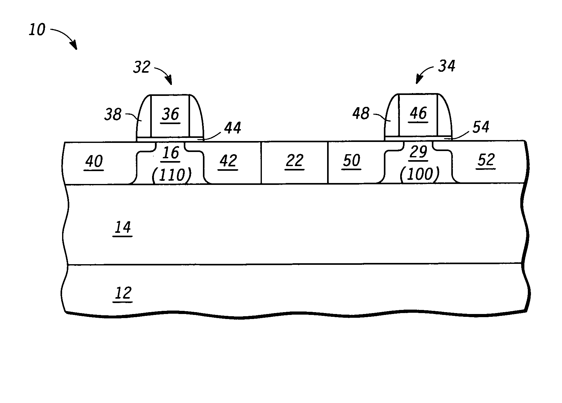
[0015]In one aspect a semiconductor device has a first semiconductor region of a first property such as a (110) surface orientation and a second semiconductor region separated from the first region by isolation. The first property is chosen to enhance the operation of a first transistor type. The second region is converted to amorphous while leaving the first region with the first property. A semiconductor layer having a second property that enhances the operation of a second transistor type is then bonded to the semiconductor device. The second region is then converted to the second property based on being bonded to the semiconductor having the second property. The semiconductor layer is removed. A transistor of the first type is formed in the first region, and a transistor of the second type is formed in the second region. This is better understood by reference to the drawings and the following description.

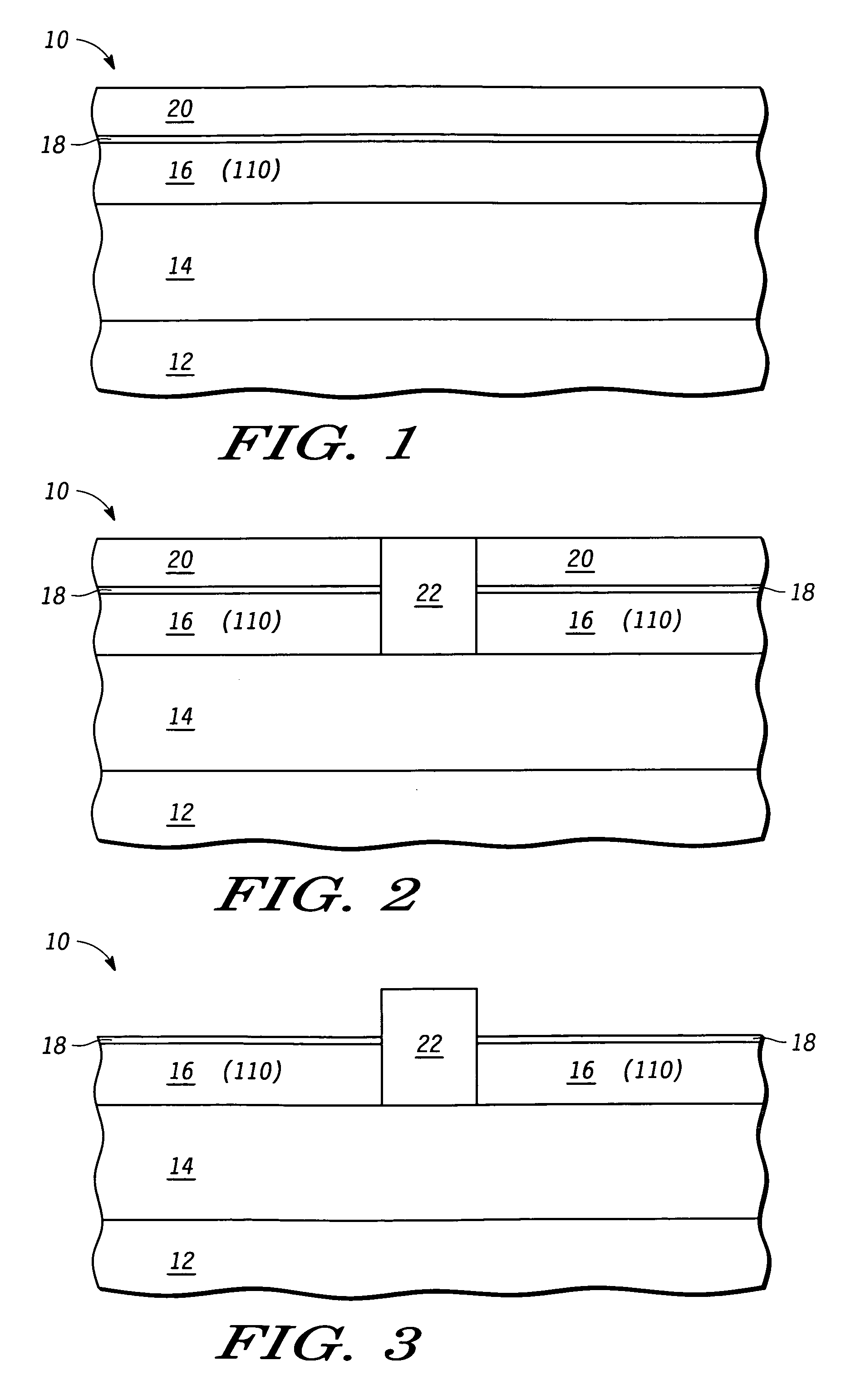
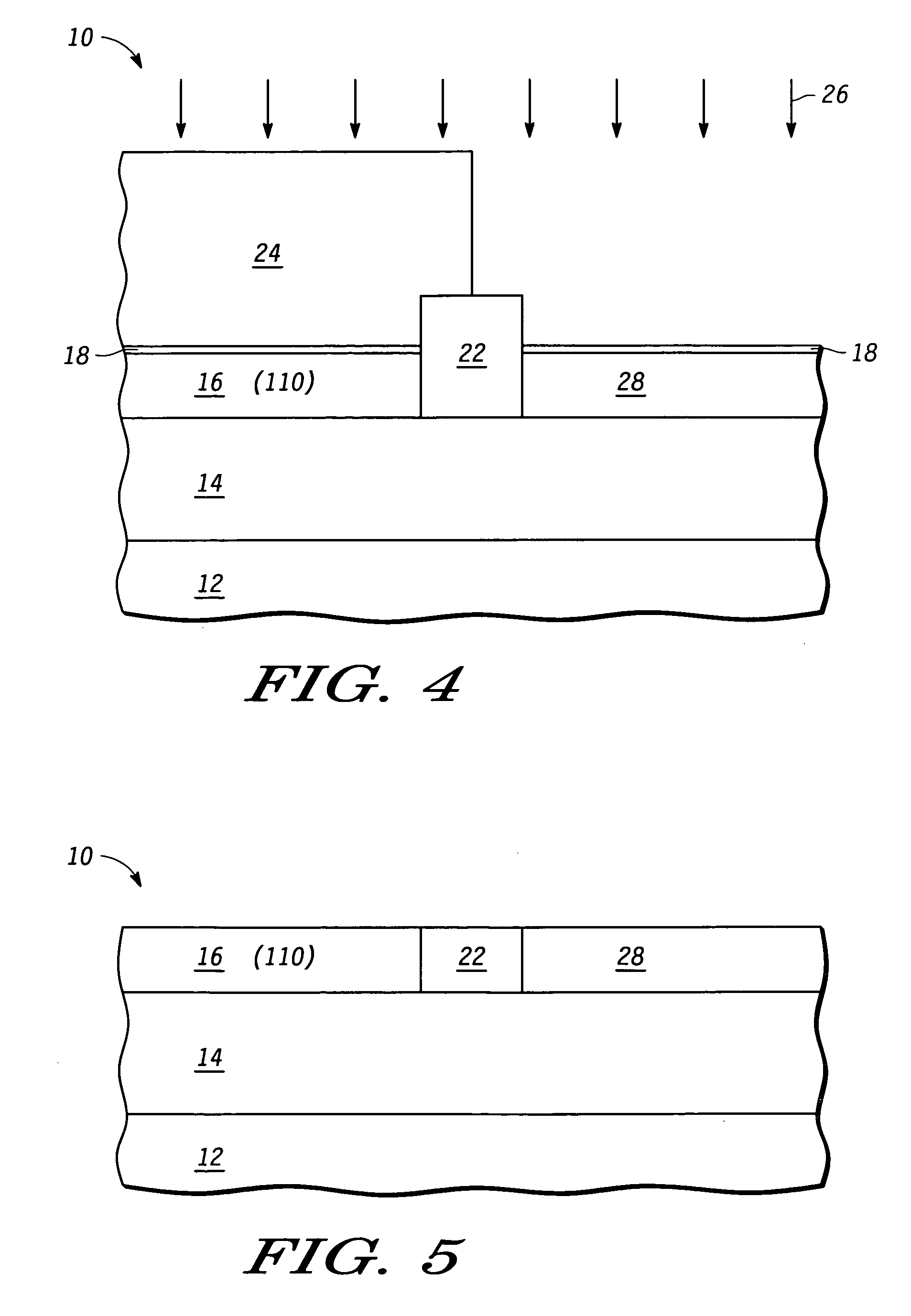
[0016]Shown in FIG. 1 is a semiconductor device structure 10 comprising a s...


PUM


Abstract

A semiconductor device is formed having two physically separate regions with differing properties such as different surface orientation, crystal rotation, strain or composition. In one form a first layer having a first property is formed on an insulating layer. The first layer is isolated into first and second physically separate areas. After this physical separation, only the first area is amorphized. A donor wafer is placed in contact with the first and second areas. The semiconductor device is annealed to modify the first of the first and second separate areas to have a different property from the second of the first and second separate areas. The donor wafer is removed and at least one semiconductor structure is formed in each of the first and second physically separate areas. In another form, the separate regions are a bulk substrate and an electrically isolated region within the bulk substrate.

Description

FIELD OF THE INVENTION[0001]The invention relates to a method of making a semiconductor device and, more particularly, to a method for selectively forming regions that have different properties.BACKGROUND OF THE INVENTION[0002]A recognition that transistors of different types have different operating characteristics based on the nature of the crystalline structure has resulted in the development of semiconductor structures that are selected based on the transistor type. For example, N channel transistors have higher carrier mobility when formed in silicon with a (100) surface orientation than in a (110) surface orientation. The opposite is true for P channel transistors. Thus, techniques have been developed for forming the N channel transistors in a (100) surface orientation and P channel transistors in a (110) surface orientation. Similarly, techniques have been developed for forming N channel transistors in silicon that is under tensile stress and P channel transistors that are un...

Claims


Application Information

Patent Timeline
Patent Type & Authority Patents(United States)
IPC IPC(8): H01L21/336
CPCH01L21/76264H01L21/823807H01L21/823878H01L27/0922H01L27/1203H01L21/84Y10S438/973
Inventor SADAKA, MARIAM G.NGUYEN, BICH-YENTHEAN, VOON-YEWWHITE, TED R.
Owner NXP USA INC
Why Eureka
Try Eureka