Method for signal extraction in a universal sensor IC

a signal extraction and sensor technology, applied in the field ofsensor data acquisition systems and methods, can solve the problems of limiting the cost efficiency of such parts, limiting the use and utilization of analog technologies, and not being able to successfully cross the 0.35 micron threshold of typical analog technologies, etc., to achieve dynamic control of the bit resolution of the signal conversion, the effect of small ic and low cos

Inactive Publication Date: 2007-10-23
SENSOR PLATFORMS
View PDF9 Cites 18 Cited by
  • Summary
  • Abstract
  • Description
  • Claims
  • Application Information

AI Technical Summary

Benefits of technology

[0007]The present invention uniquely addresses this issue of universality, thereby allowing the manifold advantages enumerated above. Not only does it simply and elegantly achieve such universality, but it also achieves it in manner that makes the solution inherently lower cost than traditional methods of signal drive and analog-to-digital conversion. It also consists of such little traditional analog circuitry that it is the only technological approach that has the capability of being transitioned to ever smaller silicon process geometries, in order to take advantage of cost, size and power consumption improvements. The present invention is a very unique approach for extracting measurable signals from sensor elements in that it is inherently more of a digital electronic solution as opposed to an analog one. As digital silicon processing techniques migrate to ever smaller line widths and geometries, i.e. 0.13 micron, 90 nm, and even 70 nm, the analog world has not been able to utilize and leverage such advances. Typical analog technologies have not successfully crossed the 0.35 micron threshold, especially for sensor applications. This limits the cost efficiency that such parts could enjoy if they were able to do so. The present invention makes it much more feasible to leverage such trends in the shrinking of silicon process geometries, thereby enabling similar or even improved performance, at ever lower costs and smaller part sizes.
[0008]The present invention is a general “one-size-fits-all” circuit that can work with any resistive, capacitive, inductive, or voltage based sensor element. This allows for a single IC that can be used across almost any sensor application. The sensor element is included as a timing element in a simple, rail to rail output, Schmitt trigger oscillator. As the sensor element's impedance varies in response to its measurand it causes the time constant of the Schmitt trigger oscillator to also vary in proportion. This causes the oscillator to output a digital-logic-level-compatible square-wave whose frequency varies as a function of the sensor elements measured. This frequency varying digital output signal is then fed into a very high resolution digital period counter in order to extract a numerical value representative of the sensor element's reading.
[0009]The advantages are numerous, including the fact that there are very few analog stages in such a topology, which keeps the IC small and low cost. Additionally, the time constant of the sensor can be matched up with a fixed impedance counterpart so that a broad variety of different sensor impedances can be accommodated. For instance, if the sensor element is a capacitive pressure sensor, it can be matched up with a resistor such that the total RC time constant of this RC-Schmitt Trigger oscillator can be centered about any conveniently desired oscillation frequency. The same applies to inductive, resistive or, in a slightly different topology, voltage-based sensors as well.

Problems solved by technology

As digital silicon processing techniques migrate to ever smaller line widths and geometries, i.e. 0.13 micron, 90 nm, and even 70 nm, the analog world has not been able to utilize and leverage such advances.
Typical analog technologies have not successfully crossed the 0.35 micron threshold, especially for sensor applications.
This limits the cost efficiency that such parts could enjoy if they were able to do so.
Also, because multiple cycles of the sensor oscillator are taken in order to extract the signal, the noise characteristics are very favorable since such averaging naturally results in digital low pass filtering.

Method used


Image

  • Method for signal extraction in a universal sensor IC
  • Method for signal extraction in a universal sensor IC
  • Method for signal extraction in a universal sensor IC

Examples


Embodiment Construction

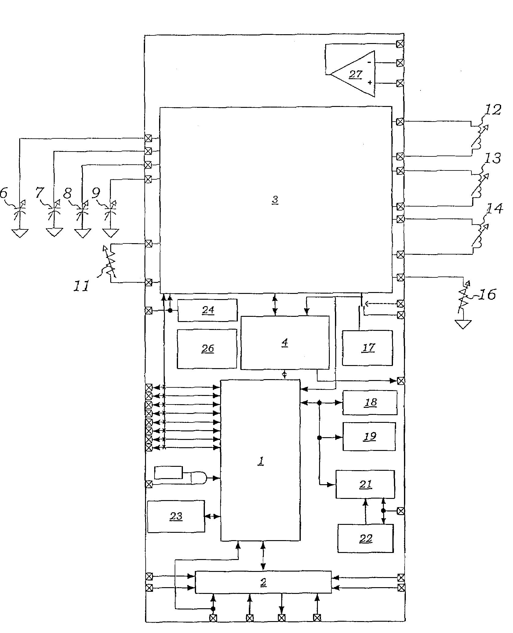
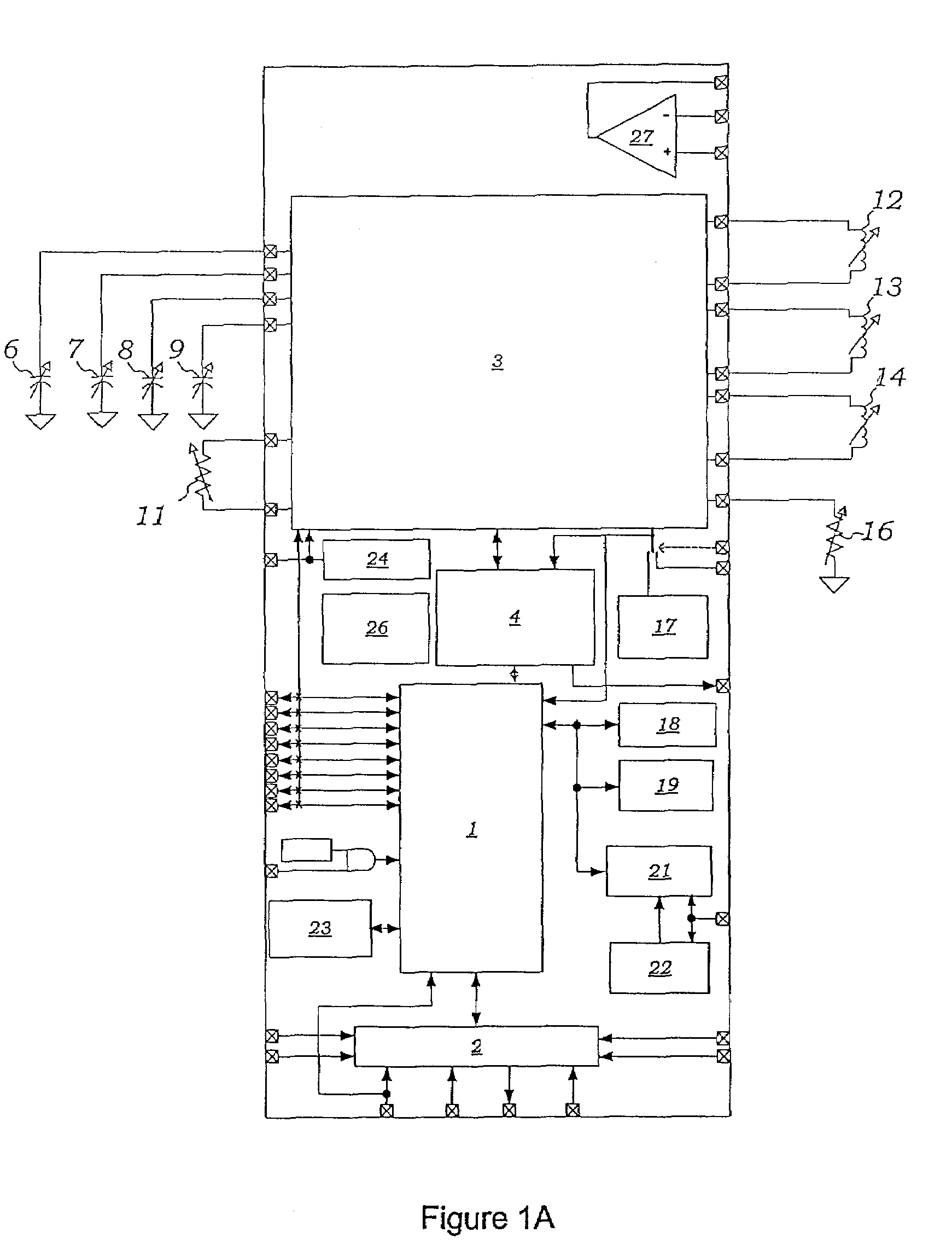
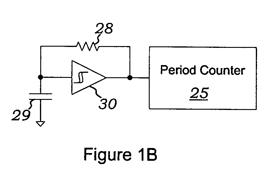
[0041]FIG. 1A is a block diagram of a first embodiment of the circuit in accordance with the present invention. A microprocessor performs most of the calculation functions of the device. A suitable microprocessor is a R80515 microprocessor but any suitable microprocessor could be substituted. An SPI and I2C (SPI / I2C) interface 2 is connected to microprocessor 1. SPI / I2C interface 2 provides suitable output signals in a variety of formats. An LR & RC Sensor Oscillator circuit 3, which is further detailed in FIG. 1B where the primary building block is a Schmitt trigger oscillator 30, is connected to microprocessor 1 by means of a Period Counter unit 4, 25. Four capacitive sensor units 6, 7, 8 and 9 and a resistive sensor 11 are shown connected to Oscillator 3 in this embodiment although it should be realized that the number of sensors necessary will vary with the application. Sensors 6, 7, 8, 9, and 11 are passive sensors connected in an RC oscillator configuration. Three inductive se...


PUM


Abstract

A apparatus and method for creating a universally usable and configurable sensor platform which is used in conjunction with various sensor and sensing elements to sense and measure environmental conditions which incorporates inputs from multiple sensors 6-9 and 12-14. The apparatus incorporates an oscillator 3 which provides a signal whose frequency varies according to the inputs from sensors 6-9 and 12-14 in combination with a microprocessor 1. A cordic block 61 allows for supplemental calculations of trigonometric operations and functions. An output unit 2 converts the signals received from microprocessor 1 into a variety of serial protocols.

Description

TECHNICAL FIELD[0001]The present invention relates to sensor data acquisition systems and methods. More particularly, the present invention relates to methods and apparatus for connecting to a wide variety of different sensors and performing signal processing to give useful information from the outputs of the sensors.BACKGROUND ART[0002]As the variety and number of sensor elements continue to be developed for the automotive, consumer, industrial and medical markets, the plethora of signal drive, acquisition and processing solutions have also likewise increased in direct proportion. Low volume applications are generally limited to custom circuits of discrete active and passive electronic components where the elements of cost, size, power consumption and reliability are poorly optimized. In higher volume applications, where the development of semi-custom or fully custom application specific integrated circuits (ASIC) can be justified from a cost and risk standpoint, the overwhelming p...

Claims


Application Information

Patent Timeline
Patent Type & Authority Patents(United States)
IPC IPC(8): G01R27/02
CPCG01D21/02
Inventor HSU, GEORGEMILLER, JOSEPH FRANK
Owner SENSOR PLATFORMS
Why Eureka
Try Eureka