Impedance control circuits and methods of controlling impedance

a technology of impedance control and impedance, applied in logic circuit coupling/interface arrangement, pulse technique, baseband system details, etc., can solve the problem that the delay circuit may delay the code value generated, and achieve the effect of reducing board size and less complicated

Active Publication Date: 2007-10-23
SAMSUNG ELECTRONICS CO LTD
View PDF13 Cites 38 Cited by
  • Summary
  • Abstract
  • Description
  • Claims
  • Application Information

AI Technical Summary

Benefits of technology

[0027]Example embodiments of the present invention provide a semiconductor device which may be less complicated and / or have reduced board size.

Problems solved by technology

The delay circuit may delay the code value generated from the code generating section by one clock cycle.

Method used


Image

  • Impedance control circuits and methods of controlling impedance
  • Impedance control circuits and methods of controlling impedance
  • Impedance control circuits and methods of controlling impedance

Examples


Embodiment Construction

[0053]Example embodiments of the present invention will become more apparent by describing, in detail, the attached drawings, wherein like elements are represented by like reference numerals, which are given by way of illustration only and thus do not limit the example embodiments of the present invention.

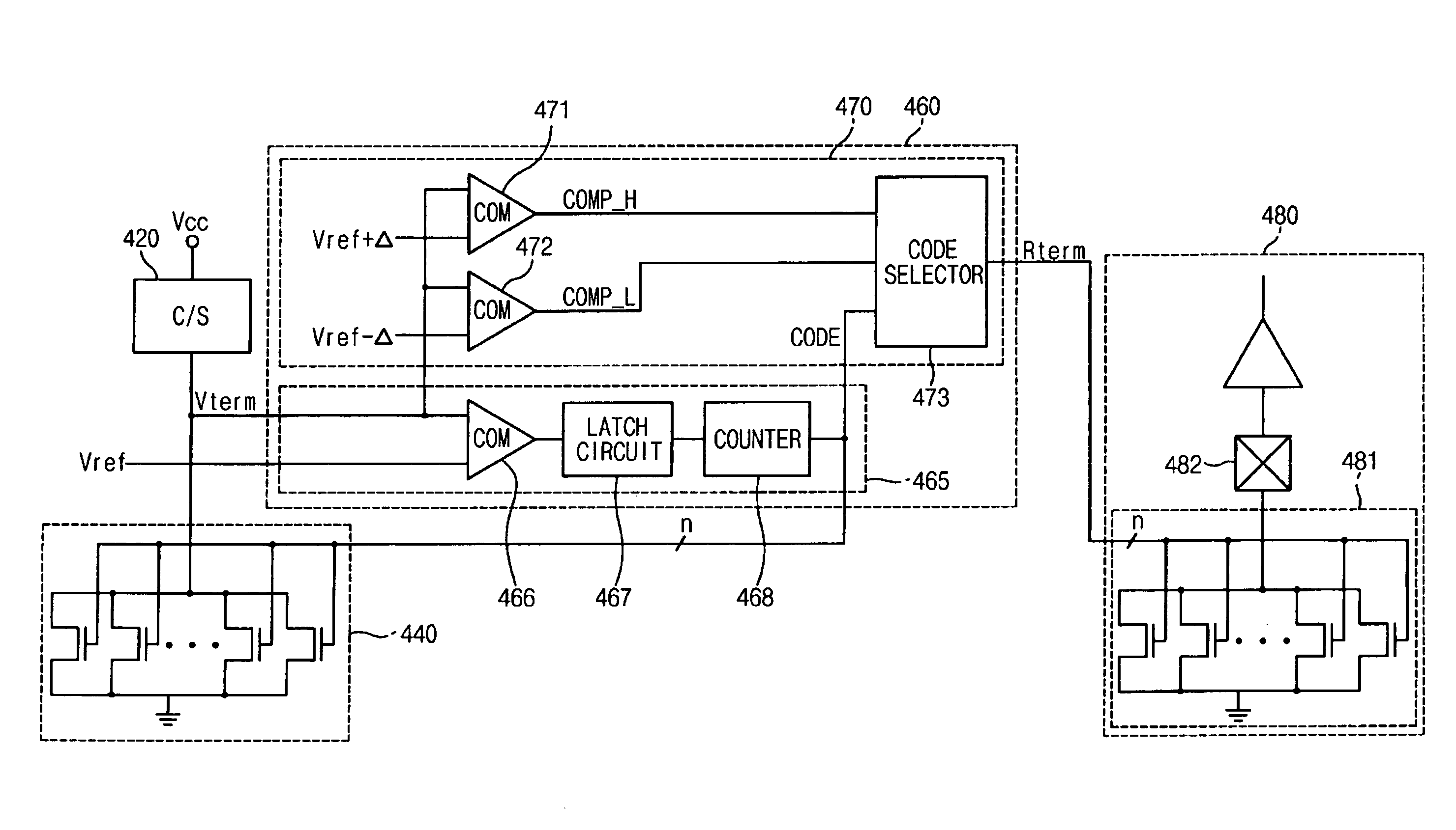
[0054]FIG. 4 is a block diagram illustrating an impedance control circuit, according to an example embodiment of the present invention.

[0055]Referring to FIG. 4, the impedance control circuit, according to an example embodiment of the present invention, may include a current source (C / S) 420, an impedance adjustment circuit 440, and a control signal generation circuit 460.

[0056]The current source 420 may be positioned in a semiconductor device and may provide a current (e.g., constant current level) to the semiconductor device.

[0057]The impedance adjustment circuit 440 may be connected, (e.g., serially connected) to the current source 420, and may control the current flowing throug...


PUM


Abstract

A circuit for controlling impedance may include an impedance adjustment circuit and a control signal generation circuit. The impedance adjustment circuit may adjust an impedance value based on a control signal. The control signal generation circuit may provide the impedance adjustment circuit with a control signal that corresponds to one of an impedance value at a first clock cycle and an impedance value at a second clock cycle that approaches a target impedance.

Description

PRIORITY STATEMENT[0001]This application claims priority under 35 USC § 119 to Korean Patent Application No. 2004-49077, filed on Jun. 28, 2004 in the Korean Intellectual Property Office (KIPO), the contents of which are herein incorporated by reference in its entirety for all purposes.BACKGROUND OF THE INVENTION[0002]1. Field of the Invention[0003]Example embodiments of the present invention relate to impedance control circuits and methods of controlling impedance.[0004]2. Description of the Related Art[0005]Related art semiconductor devices may be mounted on, for example, a board (e.g., a printed circuit board (PCB) flexible PCB, etc.). If an impedance of the board is different from that of the semiconductor device(s), data transmitted from the semiconductor devices to the board may become distorted.[0006]A resistor may be positioned outside, and connected to the semiconductor device, and an impedance control circuit may be positioned within the semiconductor device to equalize th...

Claims


Application Information

Patent Timeline
Patent Type & Authority Patents(United States)
IPC IPC(8): H03K17/16H03K19/003H01P5/12H03K5/08H04L25/02
CPCH04L25/0278H03K5/082H03H11/28
Inventor KIM, JONG-SEOK
Owner SAMSUNG ELECTRONICS CO LTD
Why Eureka
Try Eureka