This helps you quickly interpret patents by identifying the three key elements:
Problems solved by technology
Method used
Benefits of technology
Benefits of technology
[0027]An object of the present invention is to provide a light emitting unit ensuring advantages comparable to those of the display unit described in the earlier invention with a structure different therefrom, and further improving the device density such as a pixel density, enhancing the connection reliability by increasing the diameter of a via-hole for wiring without excessively reducing the size of each chip, facilitating the handling of each chip at the time of bonding by increasing the apparent area of each chip (or device), reducing the required specification in terms of alignment accuracy of each chip (or device), and to provide a double-side light emitting unit being easier for each chip (or device) and a drive control device such as a pixel transistor to be arrayed.
Problems solved by technology
Such an image display unit 10, however, fails to increase the module density per unit area because of a large occupied area of the LED modules 2.
Such a configuration of the image display unit 10 has an inconvenience that the pixel density cannot be increased due to not only the occupied area of the LED modules 2 but also the occupied area of the pixel transistor 5.
Even if the pixel transistor 4 is disposed at the periphery of an image region, there is a limitation to improvement of the pixel density because of provision of a wiring region or the like.
The display unit described in the earlier invention having the above-described advantages, however, has a problem to be improved.
Even if the pixel transistor is disposed at the periphery of an image region, there is a limitation to improvement of the pixel density because of provision of a wiring region or the like.
Another disadvantage of the display unit described in the earlier invention is that since there is a limitation to the area of a panel (area of an image portion) of the display unit, the size of each chip 40 must be reduced due to the occupied area of the pixel transistor.
Method used
Image
Click on the blue label to locate the original text in one second.
Reading with bidirectional positioning of images and text.
Examples
first embodiment
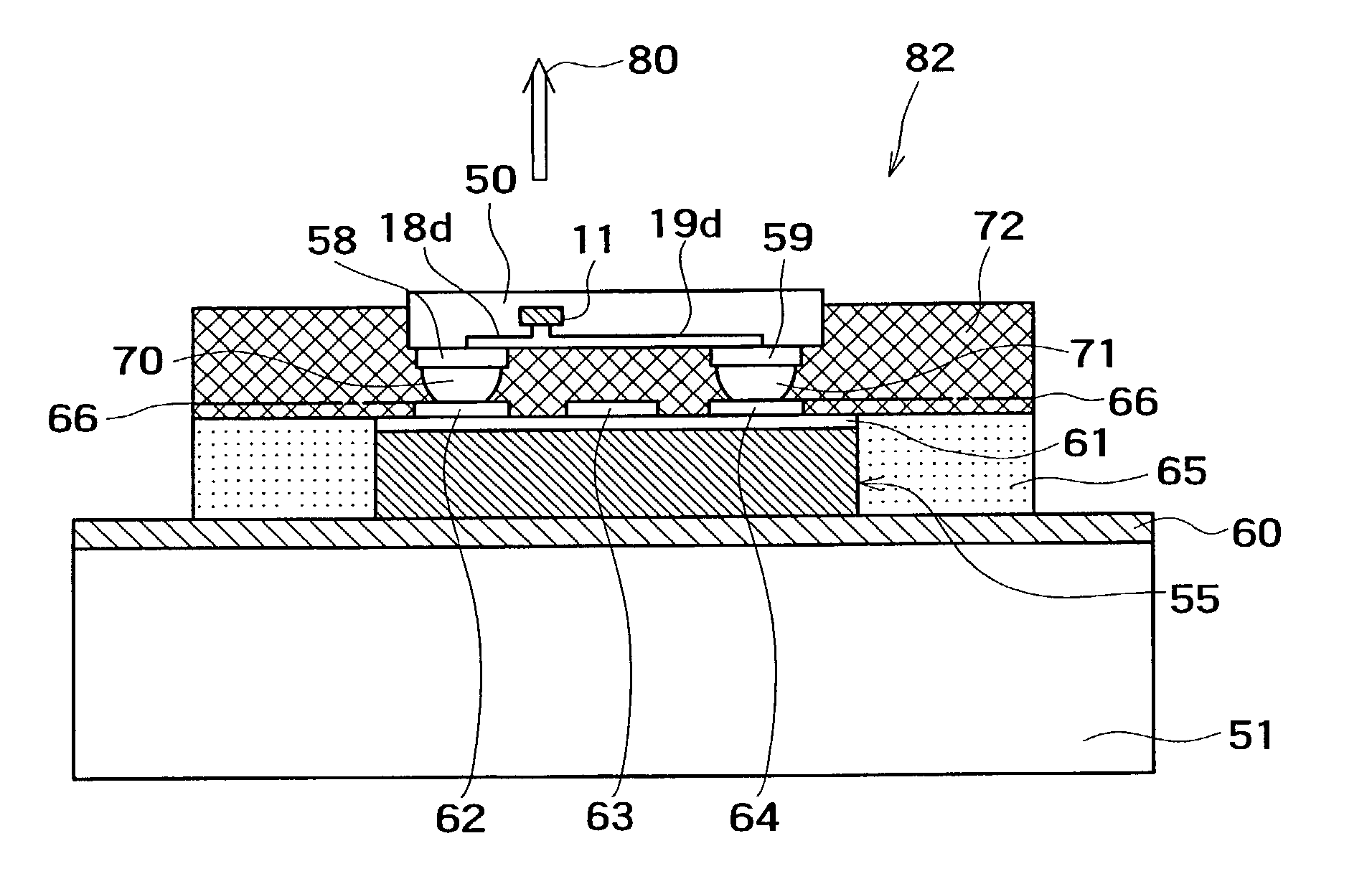
[0060]A light emitting unit represented by a display unit according to a first embodiment will be described with reference to FIGS. 1 to 5B.
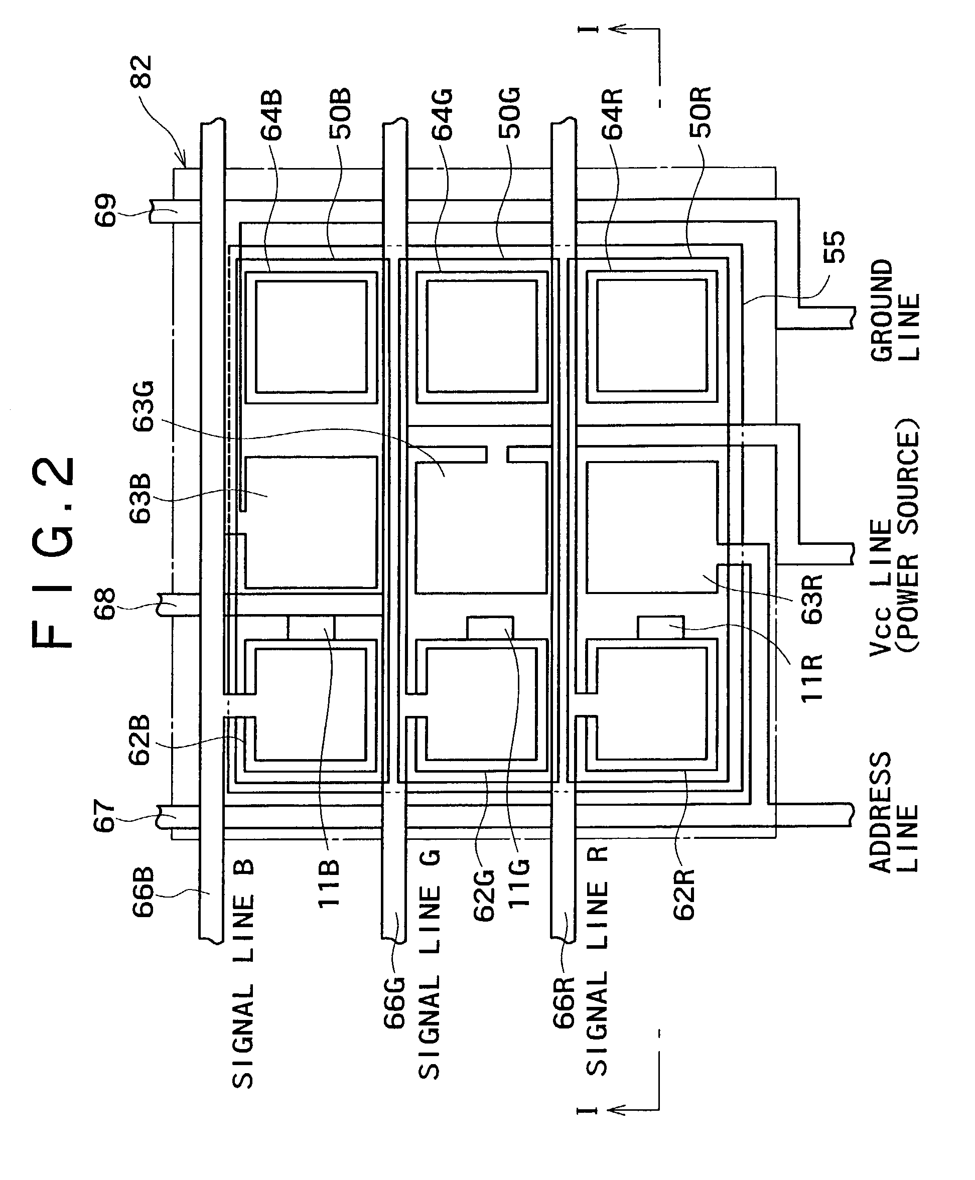
[0061]As shown in FIG. 1, a drive transistor 55 for pixel control is mounted face-up on a drive circuit board or wiring board 51 made from glass or plastic by die-bonding using a die bonding material 60. An insulating layer 61 is formed on the drive transistor 55, followed by stacked wiring, to form pads 62, 63 and 64. These pads 62, 63 and 64 are formed for re-wiring and are, as shown in FIG. 2, taken as a pad 62 for a signal line (p-side electrode), a pad 63 for an address line, a power source line, or a ground line, and a pad 64 for an n-side electrode, respectively. An insulating layer 65 is formed so as to surround the transistor 55, with wiring lines 66, 67, 68, and 69 being formed on the insulating layer 65. These lines 66, 67, 68, and 69 extend from the pads 62 and 63 of each of a number of the transistors 55 for connecting the number of...
second embodiment
[0077]A light emitting unit represented by a display unit according to a second embodiment will be described with reference to FIG. 6.
[0078]As shown in FIG. 6, the light emitting unit according to this embodiment has a structure different from that of the light emitting unit according to the first embodiment shown in FIGS. 1 and 2 in that the positional relationship between a resin-covered chip 50 in which a semiconductor light emitting device 11 is buried and a drive transistor 55 for driving the chip 50 according to this embodiment is vertically reversed to the positional relationship therebetween according to the first embodiment. Concretely, according to this embodiment, the chip 50 is disposed on the lower side (transparent substrate 51 side), and the drive transistor 55 is disposed on the upper side.
[0079]With this configuration, light rays 80 emitted from the semiconductor light emitting device 11 can be emerged through the transparent substrate 51, so that the plane of the s...
third embodiment
[0081]A light emitting unit represented by a display unit according to a third embodiment will be described with reference to FIG. 7.
[0082]The light emitting unit according to this embodiment has a structure different from that of the light emitting unit according to the first embodiment shown in FIGS. 1 and 2 in that resin-covered chips 50R, 50G, and 50B for emission of light of red, green, and blue, respectively, are not disposed side by side on one plane, but are vertically overlapped to each other above a drive transistor 55 in such a manner that semiconductor light emitting devices 11R, 11G, and 11B buried in the chips 50R, 50G, and 50B, respectively, are offset from each other. It is to be noted that in FIG. 7, the connection between each extraction electrode and the drive transistor 55 is shown only for the device 11R for emission of red light. For each of the devices 11G and 11B for emission of light of green and blue, the connection between each extraction electrode and the...
PUM
Abstract
A light emitting unit represented by an image display unit includes chips, each of which is formed by burying a light emitting device such as a GaN based semiconductorlight emitting device in a resin, wherein external terminals connected to the light emitting device buried in each chip are provided on the chip, and a drive control device such as a pixel transistor for controlling the drive of the light emitting device are connected to the external terminals in a state being at least partially overlapped to the chip. Such an image display unit is advantageous in improving a device density such as a pixel density, enhancing the connection reliability by increasing the diameters of via-holes for wiring without excessively reducing the size of each chip, improving the fabrication yield, facilitating the handling of the chip (or device) at the time of bonding by increasing the apparent area of the chip (or device), and lowering the required specification in terms of alignment accuracy of the chip (or device).
Description
BACKGROUND OF THE INVENTION[0001]The present invention relates to a light emitting unit suitable as an image display unit or the like.[0002]Light emitting diodes (LEDs) have been used as pixels of a light emitting unit such as an image display unit or a light source unit.[0003]FIG. 10 shows a related art image display unit 10 of this type, wherein LED modules 2 are two-dimensionally arrayed on and fixed to a base body 1, and an anodeelectrode 3 and a cathodeelectrode 4 of each of the LED modules 2 are connected to wiring lines on the base body 1 by wire bonding or soldering.[0004]The image display unit 10 has a screen including, for example, several hundreds of thousand pixels, wherein each of LED chips cut off from a wafer is used as the LED module 2 constituting one pixel. Such an image display unit 10, however, fails to increase the module density per unit area because of a large occupied area of the LED modules 2.[0005]FIG. 11 is a plan view showing an essential portion of the...
Claims
Application Information
Patent Timeline
Application Date:The date an application was filed.
Publication Date:The date a patent or application was officially published.
First Publication Date:The earliest publication date of a patent with the same application number.
Issue Date:Publication date of the patent grant document.
PCT Entry Date:The Entry date of PCT National Phase.
Estimated Expiry Date:The statutory expiry date of a patent right according to the Patent Law, and it is the longest term of protection that the patent right can achieve without the termination of the patent right due to other reasons(Term extension factor has been taken into account ).
Invalid Date:Actual expiry date is based on effective date or publication date of legal transaction data of invalid patent.

