High voltage generating circuit preserving charge pumping efficiency

a high-voltage generating circuit and pumping efficiency technology, which is applied in the field of semiconductor integrated circuits, can solve the problems of slow performance of dram circuits, and achieve the effect of maintaining the pumping efficiency of high-voltage generating circuits and conserving charge pumped

Inactive Publication Date: 2007-11-13
SAMSUNG ELECTRONICS CO LTD
View PDF10 Cites 2 Cited by
  • Summary
  • Abstract
  • Description
  • Claims
  • Application Information

AI Technical Summary

Benefits of technology

[0012]The present invention provides a high voltage generating circuit capable of improving charge pumping efficiency at a high power supply voltage and at a low power supply voltage.
[0025]Accordingly, a high voltage generating circuit according to the present invention is capable of conserving charge pumped to a node by isolating a current path between a power supply voltage and the node when the power supply voltage is smaller than a voltage apparent at the node, thereby maintaining the pumping efficiency of the high voltage generating circuit. Since the voltage apparent at the node is maintained during a precharge period, the pumping efficiency during subsequent periods is also maintained.

Problems solved by technology

A high-density Dynamic Random Access Memory (DRAM) typically operates at a low power supply voltage of 1.5 V or 1.8 V. Unfortunately, the low power supply voltage tends to cause sluggishness in the performance of the DRAM circuit.

Method used


Image

  • High voltage generating circuit preserving charge pumping efficiency
  • High voltage generating circuit preserving charge pumping efficiency
  • High voltage generating circuit preserving charge pumping efficiency

Examples


Embodiment Construction

[0039]The present invention will now be described more fully with reference to the accompanying drawings, in which several exemplary embodiments of the present invention are shown. Throughout the drawings and the written disclosure, like reference numerals are used to refer to like elements.

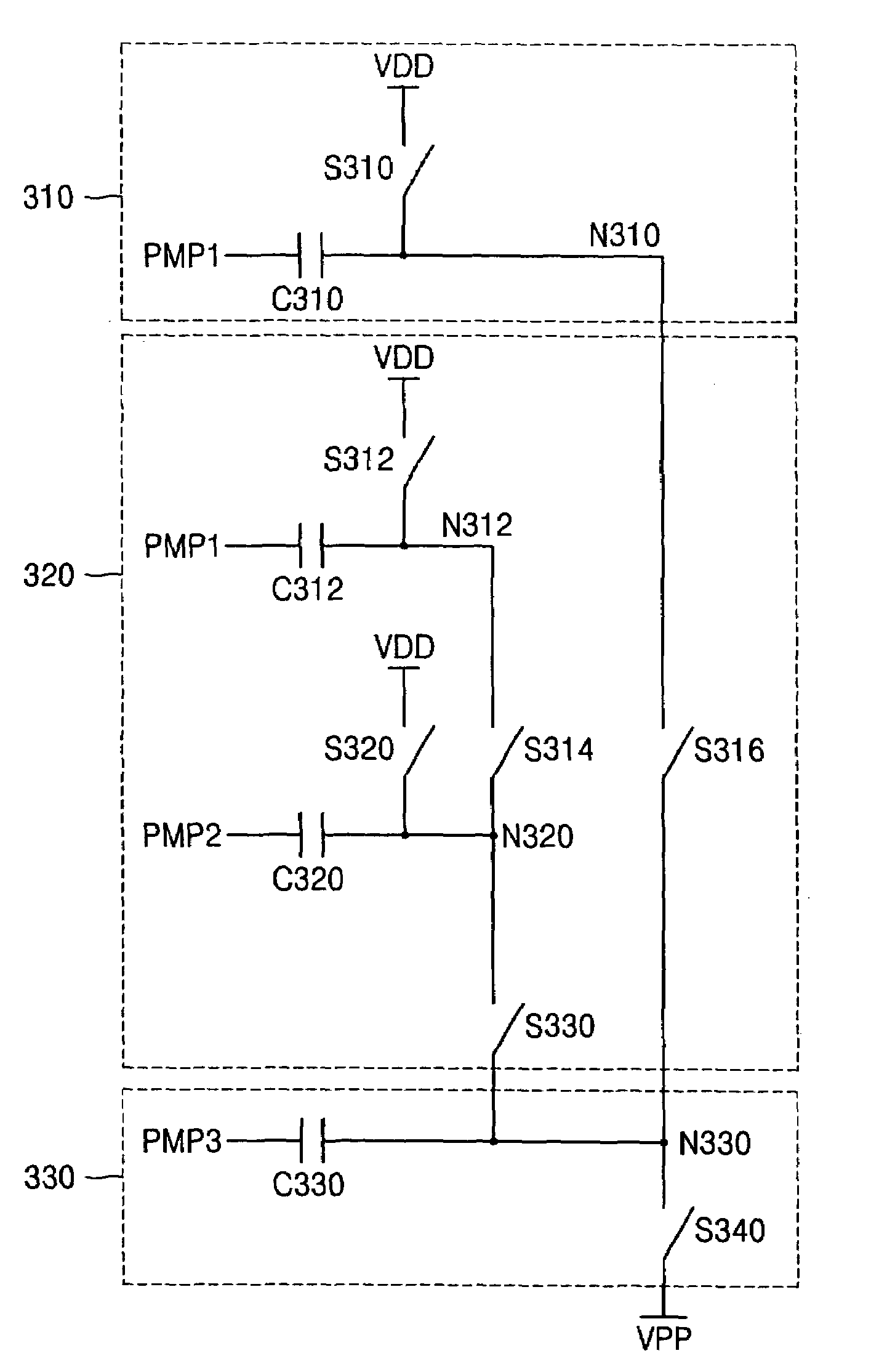
[0040]FIG. 3 is a circuit diagram for a high voltage generating circuit according to one embodiment of the present invention. The high voltage generating circuit in FIG. 3 comprises first through third pump circuits 310, 320, and 330. First through third pump circuits sequentially pump charge in order to generate a high voltage VPP, which is larger than a power source voltage VDD provided by a power source. First through third pump circuits 310, 320, and 330 collectively comprise first through fourth capacitors C310, C312, C320, and C330, first through seventh switches S310, S312, S314, S316, S320, S330, and S340, first through fourth boost nodes N310, N312, N320, and N330, and the power supply.

[...


PUM


Abstract

A high voltage generating circuit is disclosed. In the high voltage generating circuit a boost node is precharged and boosted by a plurality of pump circuits and then discharged to an output terminal. Where a voltage apparent at the boost node is smaller than a power supply voltage, the voltage apparent at the boost node is elevated to the power supply voltage. Where the voltage apparent at the boost node is larger than the power supply voltage, a current path is prevented from forming between the boost node and the power supply voltage so as to maintain the voltage apparent at the boost node.

Description

BACKGROUND OF THE INVENTION[0001]1. Field of the Invention[0002]The present invention relates generally to a semiconductor integrated circuit, and more particularly, to a high voltage generating circuit preserving charge pumping efficiency.[0003]A claim of priority is made to Korean Patent Applications No. 10-2004-0024893 and No. 10-2004-0037688, filed respectively on Apr. 12, 2004 and May 27, 2004. The disclosures of these Korean Applications are incorporated herein by reference in their entirety.[0004]2. Description of the Related Art[0005]A high-density Dynamic Random Access Memory (DRAM) typically operates at a low power supply voltage of 1.5 V or 1.8 V. Unfortunately, the low power supply voltage tends to cause sluggishness in the performance of the DRAM circuit. For example, the low power supply voltage generally causes sense amplifiers to operate slowly and bit lines to precharge slowly. In order to address these and other issues, a DRAM typically provides a boosted voltage o...

Claims


Application Information

Patent Timeline
Patent Type & Authority Patents(United States)
IPC IPC(8): G05F1/10G11C5/14G11C7/00H02M3/07G11C7/12G11C11/407G11C11/4074G11C16/06
CPCG11C5/145H02M3/07G11C11/4074
Inventor KOOK, JEONG-HOONLEE, JUNG-HWAKIM, JUNG-SUKKIM, DAE-HWAN
Owner SAMSUNG ELECTRONICS CO LTD
Why Eureka
Try Eureka