Organic electro-luminescent device, manufacturing method for the same, and electronic equipment

a technology of electroluminescent devices and manufacturing methods, applied in the direction of identification means, instruments, liquid/solution decomposition chemical coatings, etc., can solve the problem of more problems of phase separation, and achieve the effect of superior display properties

Inactive Publication Date: 2007-11-27
SEIKO EPSON CORP
View PDF22 Cites 26 Cited by
  • Summary
  • Abstract
  • Description
  • Claims
  • Application Information

AI Technical Summary

Benefits of technology

[0023]According to the present invention, it is possible to provide electronic equipment that is equipped with a display apparatus having superior display properties.

Problems solved by technology

It was observed that problems of the phase separation occur more easily with compositions including a larger number of organic electro-luminescent materials, and thus in the discharge formation of a layer, those compositions including a larger number of organic electro-luminescent materials are processed after the compositions comprising a fewer number of organic electro-luminescent materials.

Method used


Image

  • Organic electro-luminescent device, manufacturing method for the same, and electronic equipment
  • Organic electro-luminescent device, manufacturing method for the same, and electronic equipment
  • Organic electro-luminescent device, manufacturing method for the same, and electronic equipment

Examples


example 1

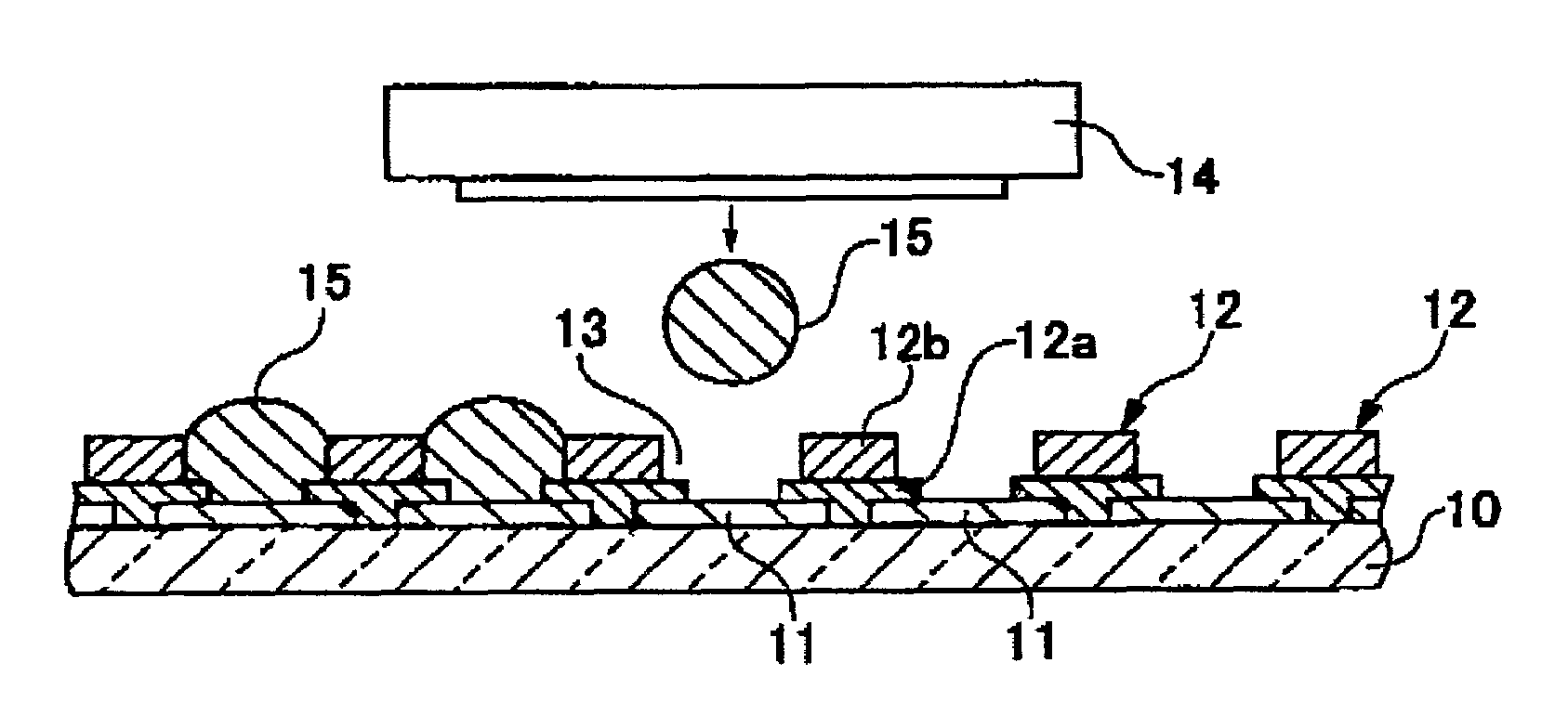
[0131]Initially, a blue light emitting layer was prepared by discharging the ink composition (blue) for a light emitting layer comprising a concentration of 1% (wt / vol) shown in Table 3, from an ink jet printer (MJ-930C manufactured by Epson) by 20 pl under an N2 gas flow, and then drying under the conditions of 25° C. and 1 atm.

[0132]Subsequently, a green light emitting layer was prepared by discharging the ink composition (green) for a light emitting layer including a concentration of 1% (wt / vol) shown in Table 2, into a neighboring opening 13 at 20 pl under an N2 gas flow, and then drying under the conditions of 25° C. and 1 atm.

example 2

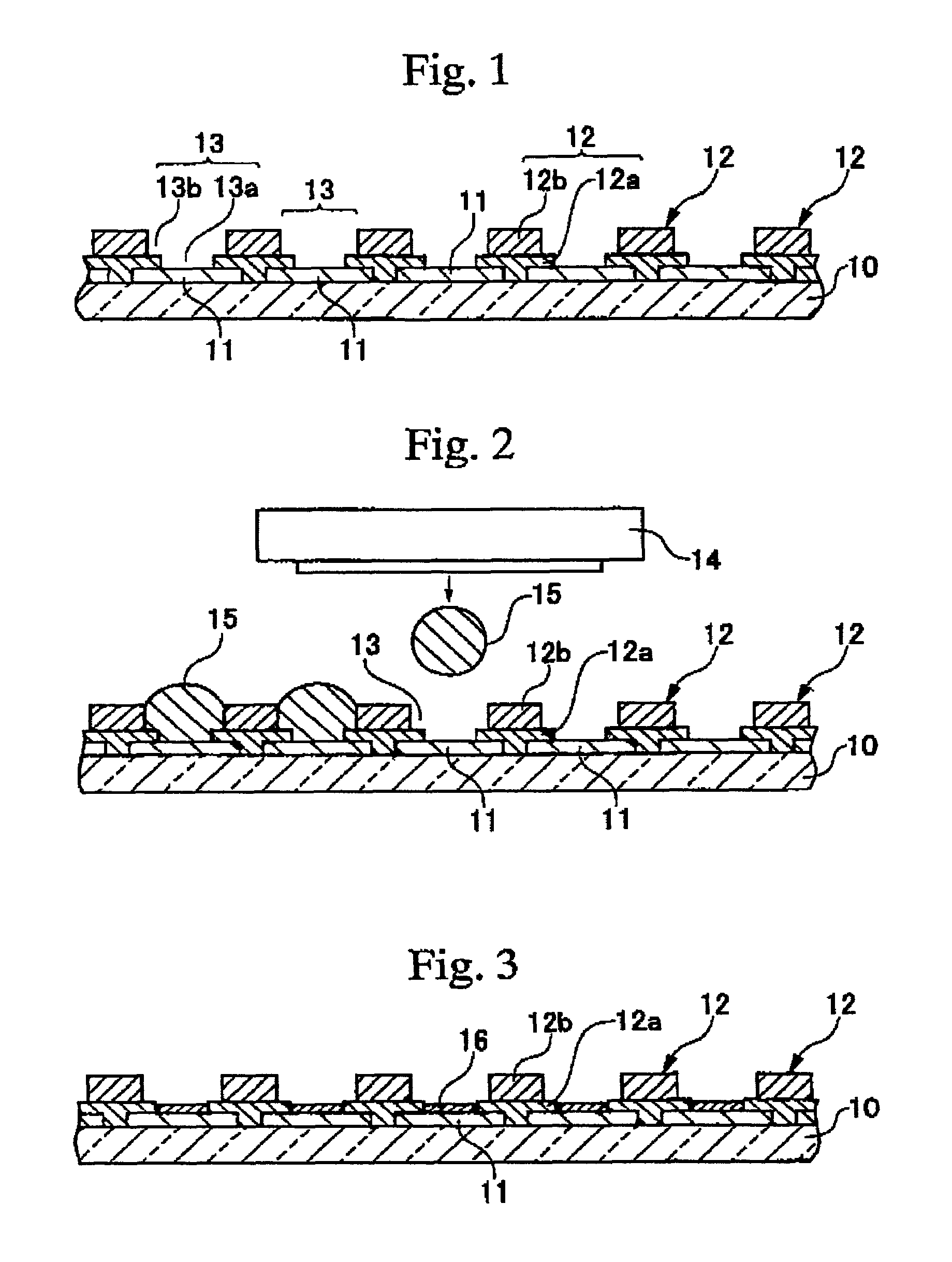
[0133]Initially, a blue light emitting layer was prepared by discharging the ink composition (blue) for a light emitting layer including a concentration of 1% (wt / vol) shown in Table 3, from an ink jet printer (MJ-930C manufactured by Epson) at 20 pl under an N2 gas flow, and then drying under the conditions of 25° C. and 1 atm.

[0134]Subsequently, a red light emitting layer was prepared by discharging the ink composition (red) for a light emitting layer including a concentration of 1% (wt / vol) shown in Table 4, into a neighboring opening 13 at 20 μl under an N2 gas flow, and then drying under the conditions of 25° C. and 1 atm.

[0135]Thereafter, a green light emitting layer was prepared by discharging the ink composition (green) for a light emitting layer including a concentration of 1% (wt / vol) shown in Table 2, into a neighboring opening 13 at 20 pl under an N2 gas flow, and then drying under the conditions of 25° C. and 1 atm.


PUM

PropertyMeasurementUnit
thicknessaaaaaaaaaa
thicknessaaaaaaaaaa
temperatureaaaaaaaaaa

Abstract

The presentation provides a manufacturing method for forming an organic electro-luminescent device by forming a homogeneous light emitting layer which does not incur phase separation. The light emitting layer is formed by discharging ink compositions formed of at least two electro-luminescent materials on the substrate following the order which starts with an ink composition which has the fewest number of organic electro-luminescent materials or which is most difficult to be phase separated.

Description

BACKGROUND OF THE INVENTION[0001]1. Field of the Invention[0002]The present invention relates to an organic electro-luminescent device provided with electric light emitting elements used for displays, and display light sources, and the like, a manufacturing method for the same, and electronic equipment.[0003]2. Description of the Related Art[0004]The development of light emitting elements using organic materials for spontaneous light emitting-type displays in place of liquid crystal displays has recently been proceeding at a rapid pace. With respect to an organic electro-luminescent device equipped with a light emitting component using an organic material in the light emitting layer, a related art method for forming a low molecular weight layer using an evaporation process is disclosed from page 913 in Appl. Phys. Lett. 51 (12), 21 Sep. 1987, and a related art method for coating a large molecular weight layer is disclosed from page 34 of Appl. Phys. Lett. 71 (1), July 1997.[0005]In ...

Claims


Application Information

Patent Timeline
Patent Type & Authority Patents(United States)
IPC IPC(8): B05D5/00H05B33/10G09F9/00G09F9/30H01L27/32H01L51/00H01L51/30H01L51/40H01L51/50H01L51/56H05B33/04H05B33/12H05B33/22
CPCH01L51/0005H01L27/3295H01L51/56H01L51/0037H10K71/135H10K59/122H10K85/1135H10K71/00
Inventor MORII, KATSUYUKISEKI, SHUNICHI
Owner SEIKO EPSON CORP
Why Eureka
Try Eureka