Laser crystallization and selective patterning using multiple beamlets

a laser crystallization and selective patterning technology, applied in the field of films processing techniques, can solve the problems of varying energy densities of semiconductor films processed using the conventional system and processes, tft devices not operating in the uniform manner from one crystallized region to another, and the next consecutive region may be visible, so as to reduce the perception of having a visible border, reduce the contrast between the two neighboring regions, and the performance of tft devices

Active Publication Date: 2007-11-27
THE TRUSTEES OF COLUMBIA UNIV IN THE CITY OF NEW YORK
View PDF124 Cites 29 Cited by
  • Summary
  • Abstract
  • Description
  • Claims
  • Application Information

AI Technical Summary

Benefits of technology

[0009]One of the objects of the present invention is to provide an improved process and system which can interpose crystallized areas from two sequential pulses (or set of pulses) on the substrate films such that the TFT devices can be situated in such areas so as to allow the neighboring regions of the thin film sample so as to have substantially the same performance of the TFT devices situated therein. Another object of the present invention is to interpose the crystallized areas of two sequential pulses (or set of pulses) in the border region between the neighboring regions of the sample so as to reduce a perception of having a visible border between the adjacent regions to reduce the contrast between the two neighboring regions.
[0010]In accordance with at least some of these objectives as well as others that will become apparent with reference to the following specification, it has now been determined that by specially dispersing the irradiation of one or more regions in the semiconductor thin film by portions of two or more different pulses (each of which has a differing fluence). It was also ascertained that dispersing the portions of two sequential beam pulses in a border region between two adjacent regions of the semiconductor thin film reduces the perception of the border between the pixels.
[0015]In a further exemplary embodiment of the present invention, the first areas are fully melted throughout their entire thickness, and the second areas are fully melted throughout their entire thickness. Also, the film sample may be translated so that the a further portion of the film sample is provided for irradiation by the first and second beamlets, the further portion being substantially adjacent to the particular portion of the film sample. The irradiation of the first and second areas can be repeated for processing the entire semiconductor thin film sample. A first edge of the further portion of the film sample can overlap a second edge of the particular portion of the film sample, and the irradiated and re-solidified areas in the first edge of the further portion may be intermingled with the re-solidified areas of the particular portion so as to prevent an overlap thereof.

Problems solved by technology

The semiconductor films processed using the conventional system and processes often suffer from varying energy densities from one irradiated region of such thin film to the next.
The problem may arise after such fabrication of the semiconductor thin film, i.e., when thin-film transistor (“TFT”) devices are placed in such areas irradiated and crystallized regions having differing energy densities.
For example, while the TFT devices placed in each of the crystallized regions (which may be uniform therein) generally have uniform characteristics and operate in a substantially the same manner within each such region, the TFT devices do not operate in the uniform manner from one crystallized region to another.
Another problem of the unintended consequence of irradiating the neighboring regions of the semiconductor thin film with pulses each having a slightly differing fluences is that a transition from the one of these regions to the next consecutive region may be visible.

Method used


Image

  • Laser crystallization and selective patterning using multiple beamlets
  • Laser crystallization and selective patterning using multiple beamlets
  • Laser crystallization and selective patterning using multiple beamlets

Examples


second embodiment

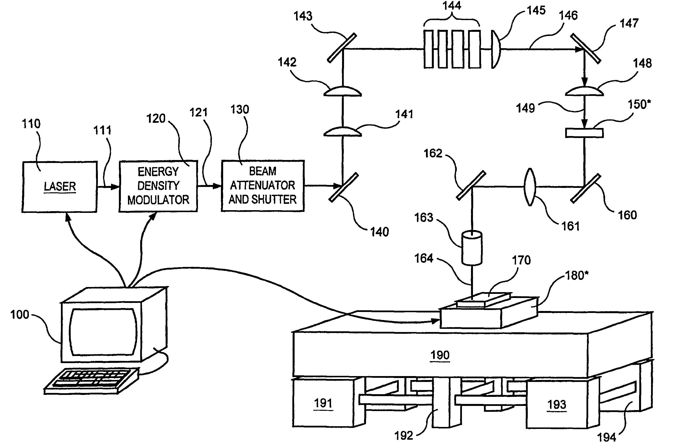
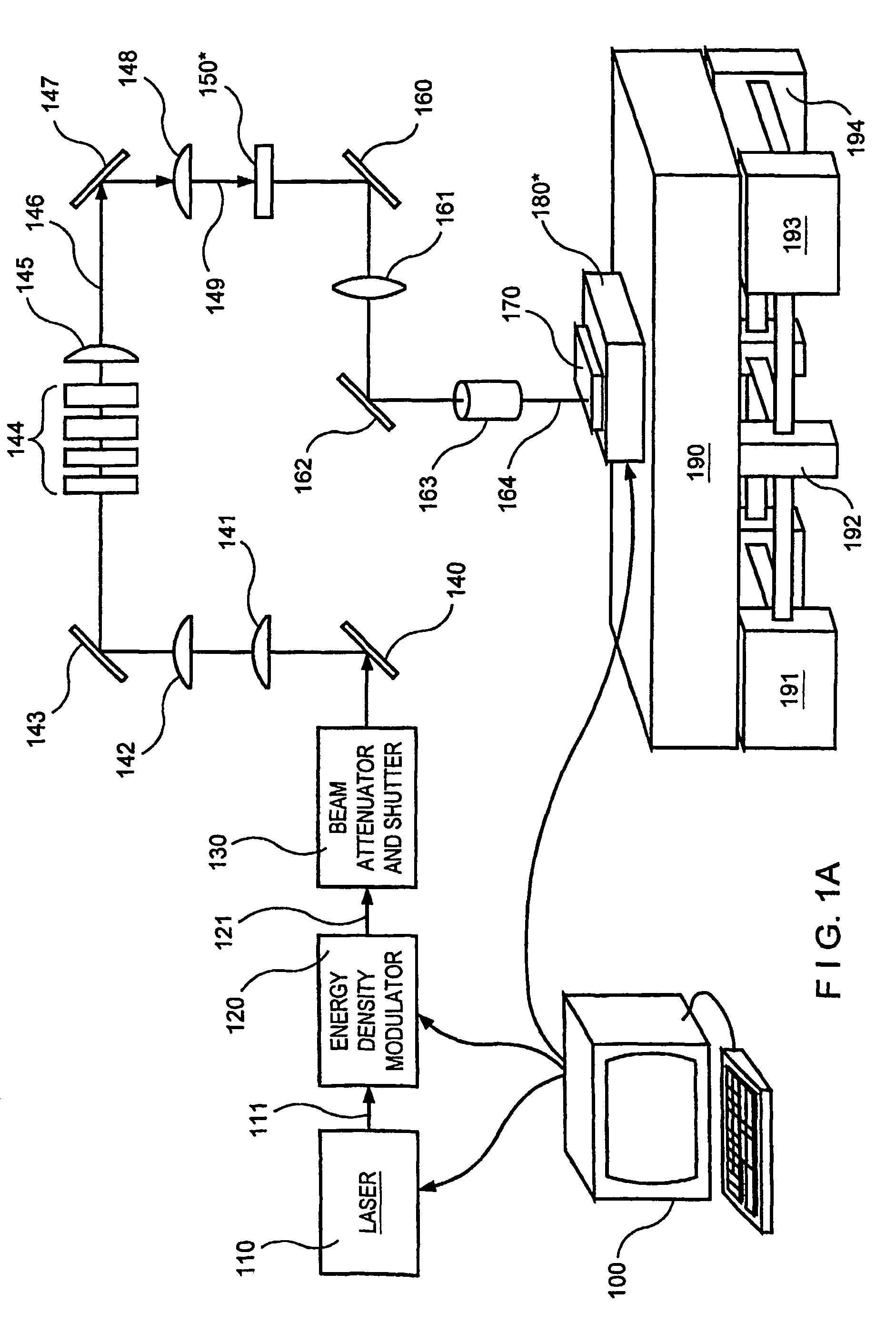
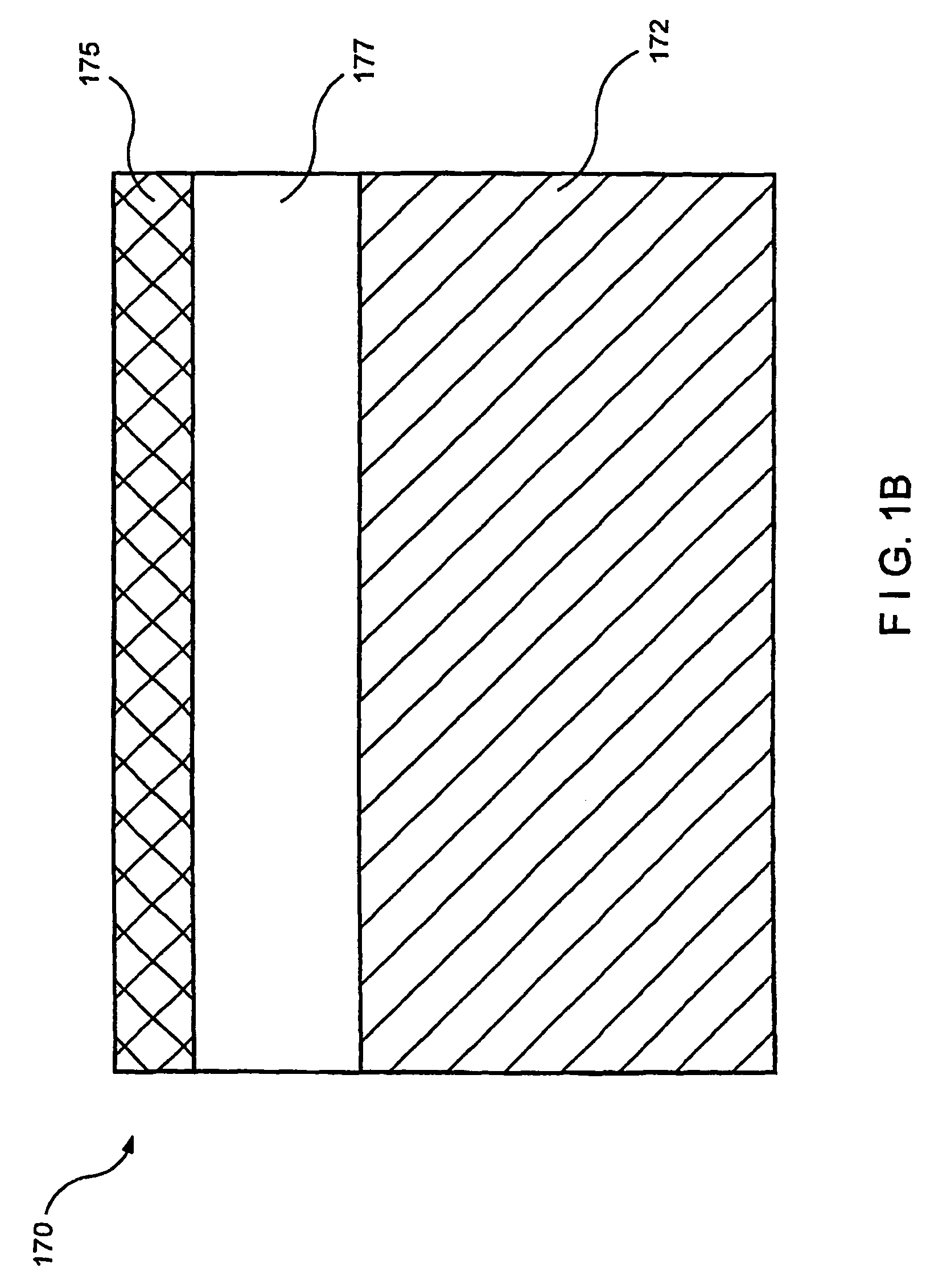
[0066]Then, when the second conceptual column 206 is started to be processed, the first one-third portion of the beam which impinges and irradiates first portions 915 of the first region 910 of this second conceptual column 206 of the semiconductor thin film 175 which were masked by the third section C′730 of the mask 150′ (see FIGS. 8F, 9F). Thus, FIGS. 8G, 8H, 9G, 9H show that the regions of the second conceptual column 206 of the semiconductor thin film 175 is irradiated by the beam pulses patterned by the mask 150′, such that the third one-third portion of the masked beam pulse 164 leads the second one-third portion of the masked beam pulse 164, which then lead the third one-third portion of the masked beam pulse 164 in their irradiation of all of the regions of the second conceptual column 206 of the semiconductor thin film 175 according to the present invention.

[0067]In this manner, all conceptual columns of the sample 170 can be properly irradiated by the beam pulses 164 that...

first embodiment

[0069]As shown in FIGS. 11A and 12A, the masked beam pulse 164 patterned by the first top section X 1000 of the mask 150″ so as to impinge and irradiate a first region 810 on the first conceptual column 205 of the semiconductor thin film sample 170, while the masked beam pulse 164 patterned by the first bottom section X′1030, the second top section Y 1050, and the second bottom section Y′1070 of the mask 150″ irradiate an area away from the edge 210′ of the semiconductor thin film 170. Therefore, as shown in FIGS. 11A and 12A, the first region 1110 of the semiconductor thin film is irradiated only by the beam pulse 164 masked by the first top section X 1000 of the mask 150″. As shown in FIG. 12A, the irradiated first region 1110 is initially composed of irradiated first portions 1112 which are provided at a distance from one another, and substantially match the positions and orientations of the slits 1010 of the first top section X 1000 of the mask 150″. As with the first embodiment...


PUM

PropertyMeasurementUnit
temperaturesaaaaaaaaaa
widthaaaaaaaaaa
lengthaaaaaaaaaa

Abstract

A process and system for processing a thin film sample, as well as the thin film structure are provided. In particular, a beam generator can be controlled to emit successive irradiation beam pulses at a predetermined repetition rate. Each irradiation beam pulse may be masked to define a first plurality of beamlets and a second plurality of beamlets. The first and second plurality of beamlets of each of the irradiation pulses being provided for impinging the film sample and having an intensity which is sufficient to at least partially melt irradiated portions of the section of the film sample. A particular portion of the section of the film sample is irradiated with the first beamlets of a first pulse of the irradiated beam pulses to melt first areas of the particular portion, the first areas being at least partially melted, leaving first unirradiated regions between respective adjacent ones of the first areas, and being allowed to resolidify and crystallize. After the irradiation of the particular portion with the first beamlets, the particular portion is again irradiated with the second beamlets of a second pulse of the irradiated beam pulses to melt second areas of the particular portion, the second areas being at least partially melted, leaving second unirradiated regions between respective adjacent ones of the second areas, and being allowed to resolidify and crystallize. The first irradiated and re-solidified areas and the second irradiated and re-solidified areas are intermingled with one another within the section of the film sample. In addition, the first areas correspond to first pixels, and the second areas correspond to second pixels.

Description

RELATED APPLICATION[0001]This application is a national phase of International Patent Application No. PCT / US03 / 025972, filed Aug. 19, 2003, published on Feb. 26, 2004 as International Patent Publication No. WO 04 / 017382, which claims priority from U.S. Provisional Application No. 60 / 405,083, which was filed on Aug. 19, 2002, each of which are incorporated by reference in their entireties herein, and from which priority is claimed.NOTICE OF GOVERNMENT RIGHTS[0002]The U.S. Government may have certain rights in this invention pursuant to the terms of the Defense Advanced Research Project Agency award number N66001-98-1-8913.FIELD OF THE INVENTION[0003]The present invention relates to techniques for processing of films, and more particularly to techniques for processing semiconductor films to spatially intermix multiple irradiations of areas of films of such thin films so as to obtain a substantial performance uniformity of electronic devices, such as thin-film transistor (“TFT”) device...

Claims


Application Information

Patent Timeline
Patent Type & Authority Patents(United States)
IPC IPC(8): H01L21/00C30B13/00C30B21/04C30B28/08H01L21/20H01L21/36B23K26/06B23K26/067H01L21/268H01L21/336H01L21/77H01L21/84H01L27/12H01L29/786
CPCB23K26/0656B23K26/067G03F7/70041G03F7/70725H01L29/78675H01L21/268H01L27/1285H01L27/1296H01L21/2026B23K26/066H01L21/02683H01L21/02686H01L21/02678H01L21/02422H01L21/02488H01L21/02532H01L21/02689H01L21/02691
Inventor IM, JAMES S.
Owner THE TRUSTEES OF COLUMBIA UNIV IN THE CITY OF NEW YORK
Why Eureka
Try Eureka