Semiconductor memory device

a memory device and semiconductor technology, applied in the direction of information storage, static storage, digital storage, etc., can solve the problems of excessively short write operation time, high power consumption of semiconductor memory cells, and inability to ensure stable data writing, etc., to achieve high-speed writing, low power consumption, and not excessively long write operation time

Inactive Publication Date: 2007-11-27
PANASONIC CORP
View PDF7 Cites 9 Cited by
  • Summary
  • Abstract
  • Description
  • Claims
  • Application Information

AI Technical Summary

Benefits of technology

[0009]Therefore, an object of the present invention is to provide a semiconductor memory device which performs write control at appropriate write timing regardless of fluctuations in properties of a memory cell caused by manufacturing error or the like.
[0019]The semiconductor memory device according to the present invention is capable of ensuring writing to all memory cells and generating a write control signal having an optimum pulse width. In other words, according to the semiconductor memory device of the present invention, a write operation is not ended before the writing to the memory cells has been completed and write operation time is not excessively longer than necessary. The semiconductor memory device according to the present invention can realize high-speed writing with low power consumption.

Problems solved by technology

In the meantime, because there are fluctuations in properties of the memory cell, which are caused by supply voltage dependency, temperature properties, and manufacturing error of respective transistors or the like comprising a memory cell, the write time fluctuates among the memory cells.
However, longer write operation time dissatisfies user's demand for high-speed writing and may cause a disadvantage that charge / discharge currents from the memory cell to a bit line pair increase, thus resulting in an increase in power consumption of the semiconductor memory cell.
On the contrary, excessively short write operation time may be likely to fail to ensure stable data writing.

Method used


Image

  • Semiconductor memory device
  • Semiconductor memory device
  • Semiconductor memory device

Examples


Embodiment Construction

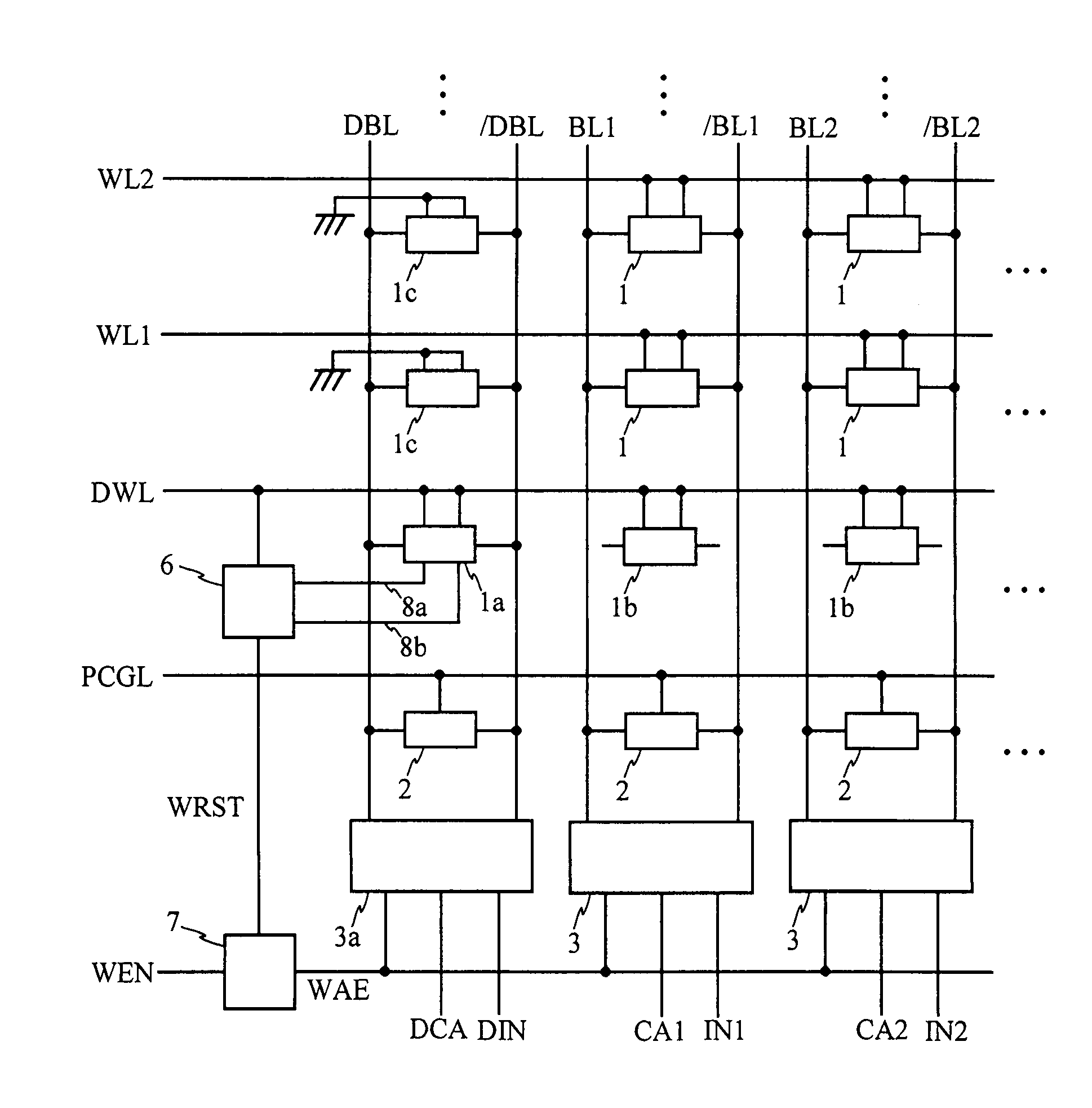
[0031]FIG. 1 is a structural diagram showing a portion of a semiconductor memory device according to the present invention. The semiconductor shown in FIG. 1 comprises memory cells 1, dummy memory cells 1a, 1b, and 1c, precharge circuit sections 2, write amplifiers 3, a dummy write amplifier 3a, a write state detection section 6, and a write amplifier control section 7.

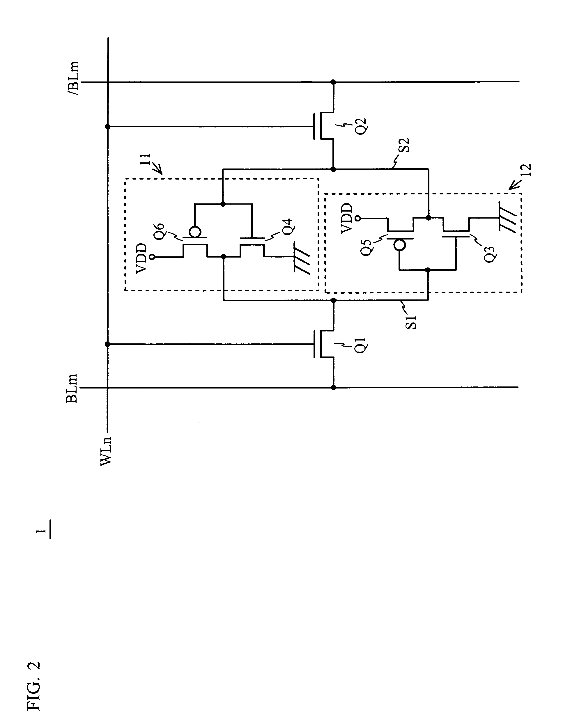
[0032]The memory cells 1 are each arranged at an intersection between a word line WLn (n is an integer more than or equal to 1) wired in a row direction and a bit line pair {BLm and / BLm} (m is an integer more than or equal to 1) wired in a column direction. The memory cells 1 arranged in a matrix manner compose a memory array section for storing information. The dummy memory cells 1a, 1b, and 1c are arranged in a circumference of the memory array section. Among the dummy memory cells, the dummy cell 1a is arranged at an intersection between a dummy word line DWL and a dummy bit line pair {DBL and / DBL}. Each of the m...


PUM


Abstract

There provided a semiconductor memory device which ensures writing to all memory cells regardless of fluctuations in properties of the memory cells caused by manufacturing error or the like and can reduce write operation time and power consumption. Write operations for a memory cell 1 and a dummy memory cell 1a are controlled based on a write amplifier control signal WAE. Write operation end timing is determined based on a write completion signal WRST which indicates a storage state of the dummy memory cell 1a. The dummy memory cell 1a and peripheral circuitry are designed so that write time required for the dummy memory cell 1a is more than or equal to a maximum of write time required for the memory cells 1.

Description

BACKGROUND OF THE INVENTION[0001]1. Field of the Invention[0002]The present invention relates to a semiconductor memory device incorporating dummy memory cells.[0003]2. Description of the Background Art[0004]In general, a semiconductor memory device comprises a memory cell array section having memory cells arrayed in a matrix manner, and peripheral circuitry. And conventionally, there has been proposed a semiconductor memory device in which dummy memory cells having the same properties as those of memory cells are incorporated beside the memory cell array section for a purpose other than information storage.[0005]Dummy memory cells are often incorporated for timing control during read processing, such as generation of a sense amplifier control signal, (for example, refer to Japanese Laid-Open Patent Publication No. 2002-367377 (FIG. 1) and Japanese Laid-Open Patent Publication No. 11-96768). A semiconductor memory device in which dummy memory cells are incorporated for timing contro...

Claims


Application Information

Patent Timeline
Patent Type & Authority Patents(United States)
IPC IPC(8): G11C7/02
CPCG11C11/413G11C11/412
Inventor YAMAGAMI, YOSHINOBU
Owner PANASONIC CORP
Why Eureka
Try Eureka