Optimization of the design of a synchronous digital circuit

a technology of synchronous digital circuit and design, which is applied in the direction of cad circuit design, program control, instruments, etc., can solve the problems of complex asic design, limited performance of this kind of circuit, and significantly lower clock frequency, so as to achieve simple and cost-effective system

Inactive Publication Date: 2007-11-27
UNWIRED PLANET
View PDF17 Cites 7 Cited by
  • Summary
  • Abstract
  • Description
  • Claims
  • Application Information

AI Technical Summary

Benefits of technology

[0011]The minimum delay value of a combinational path can often be increased easily, and thus this is a very simple way of reducing the difference between the maximum delay value and the minimum delay value. Since the greatest one of these difference values can be shown to be the lower limit for the usable clock period, a reduction will allow a shorter clock period and thus a higher clock frequency of the circuit.
[0013]When the step of increasing the minimum delay value for a combinational path is performed by inserting a number of buffers in the combinational path, a very simple and cost effective method is achieved.
[0016]When the system comprises means for identifying the combinational path having the greatest difference between the maximum delay value and the minimum delay value, and means for reducing said difference between the maximum delay value and the minimum delay value by increasing the minimum delay value for said combinational path having the largest difference, the system will be able to increase the clock frequency of a synchronous digital circuit in a relatively simple way without the use of the very complex or power consuming methods mentioned above. The minimum delay value of a combinational path can often be increased easily, and thus this is a very simple way of reducing the difference between the maximum delay value and the minimum delay value. Since the greatest one of these difference values can be shown to be the lower limit for the usable clock period, a reduction will allow a shorter clock period and thus a higher clock frequency of the circuit.
[0018]When the system is adapted to increase the minimum delay value for a combinational path by the insertion of a number of buffers in the combinational path, a simple and cost effective system is achieved.

Problems solved by technology

However, the performance of this kind of circuit is limited by the longest combinatorial delay among local paths between any pair of storage elements.
However, complex ASIC designs are rarely suitable for this method, since their data flow is complex and irregular.
However, practice has shown that the highest obtainable clock frequency is considerably lower than the theoretical limit, because it is also limited by other factors.
This relocation of registers is a very complex process for complicated circuits, because the relocation of a register typically requires the use of several new registers to replace the one that was relocated.

Method used


Image

  • Optimization of the design of a synchronous digital circuit
  • Optimization of the design of a synchronous digital circuit
  • Optimization of the design of a synchronous digital circuit

Examples


Embodiment Construction

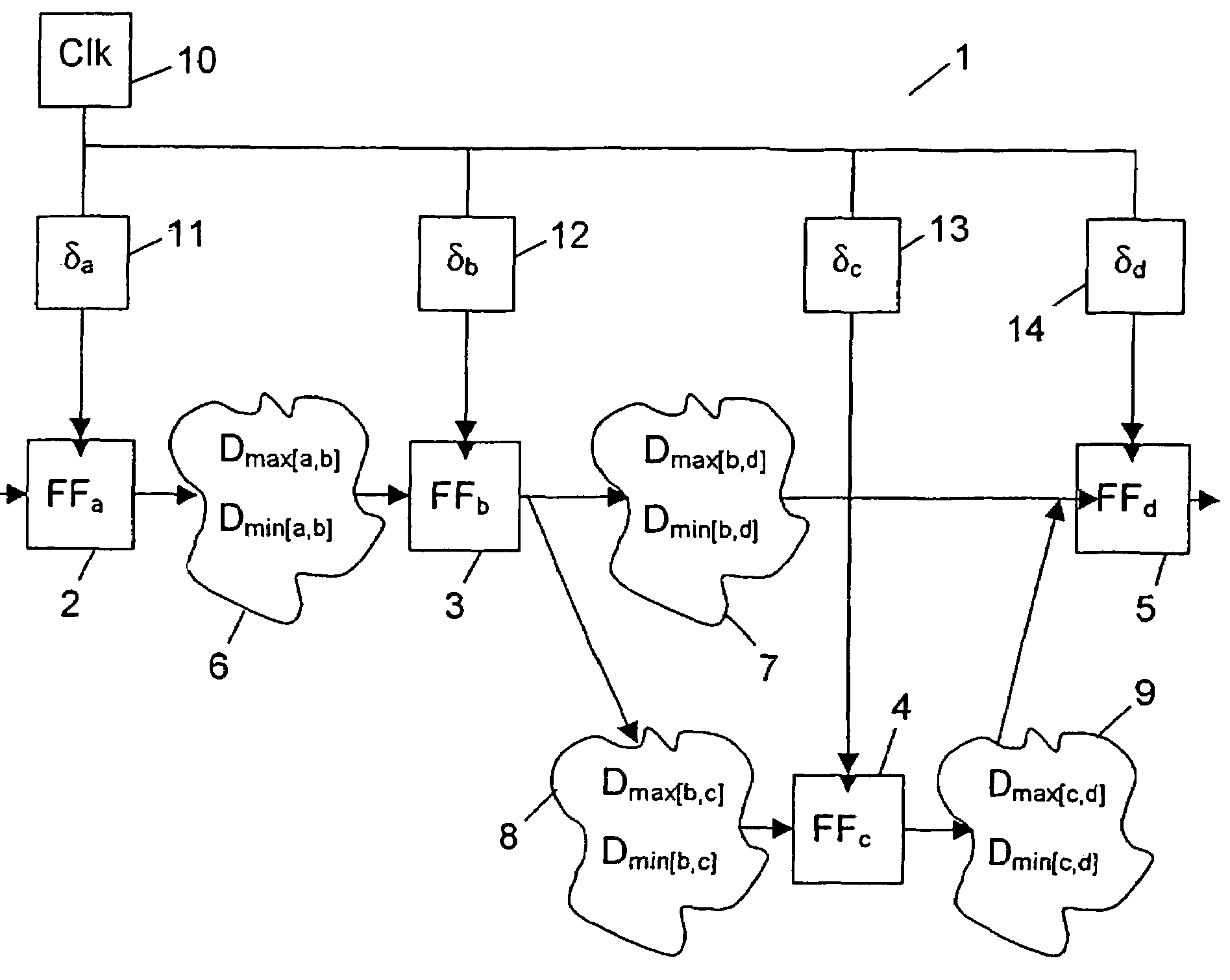
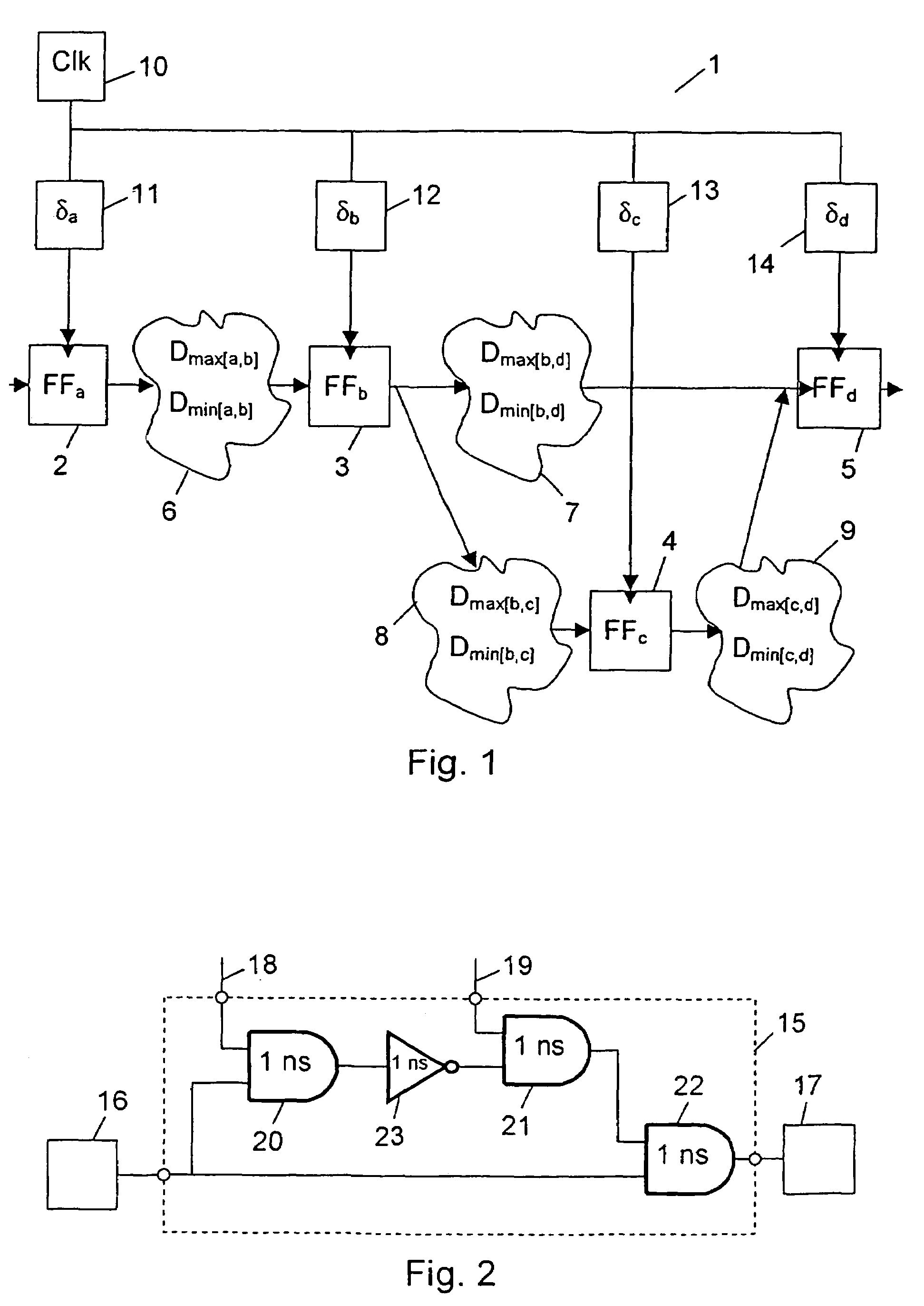
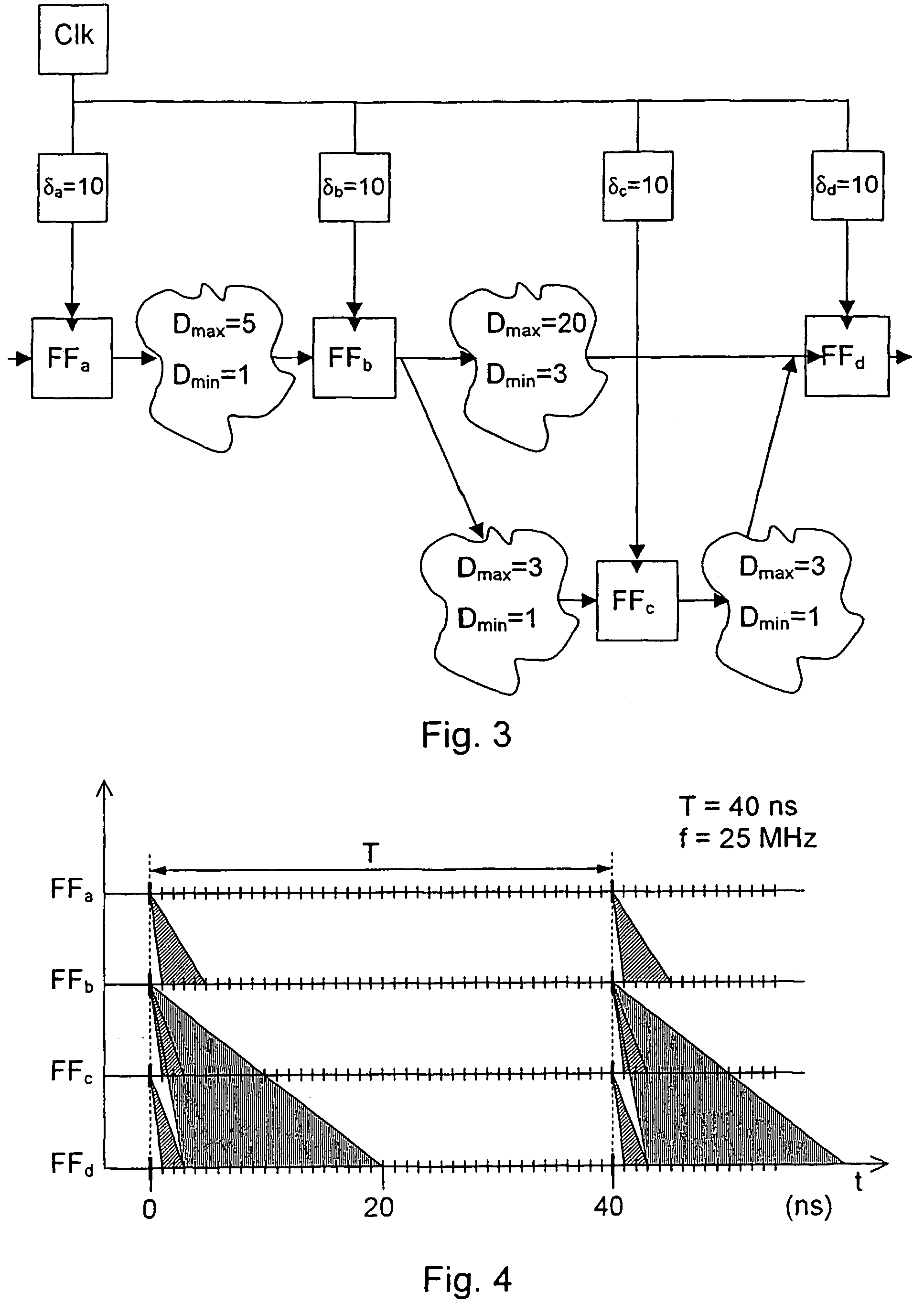
[0046]FIG. 1 illustrates an example of a synchronous digital circuit 1 having four registers 2, 3, 4, and 5 and four blocks of combinational logic 6, 7, 8 and 9. The registers 2, 3, 4, and 5 are also designated FFa, FFb, FFc and FFd, and they are clocked from a clock source 10. The clock is subjected to certain insertion delays δa, δb, δc and δd, indicated by the delay blocks 11, 12, 13 and 14, as it is distributed to the registers.

[0047]Each of the combinational logic blocks 6, 7, 8 and 9 delays the digital signals passing through them. The delay of a combinational logic block, i.e. the delay from the output of one register to the input of another register, may vary between a shortest combinational delay Dmin and a longest combinational delay Dmax. Thus the delay of e.g. the block 6, i.e. the delay from the output of register FFa to the input of register FFb, may vary between a shortest combinational delay Dmin[a,b] and a longest combinational delay Dmax[a,b].

[0048]Very often Dmin ...


PUM


Abstract

The design of a synchronous digital circuit (1) can be modified. The circuit comprises a number of clocked storage devices (2, 3, 4, 5,) and a number of combinational logic elements defining combinational paths (6, 7, 8, 9,) between at least some of said clocked storage devices. Each combinational path from an output of one clocked storage device to an input of another has a minimum delay value (Dmin) and a maximum delay value (Dmax). The actual delay of the path assumes a value between the minimum and maximum delay values. The method comprises the steps of identifying the path (6; 7; 8; 9) having the greatest difference between the maximum delay value (Dmax) and the minimum delay value (DMIN), and reducing said difference by increasing the minimum delay value for the path having the greatest difference. With the method a higher clock frequency for the circuit can be achieved.

Description

[0001]This application is a national stage application of PCT International Application No. PCT / EP02 / 10750, filed 26 Sep. 2002, which claims priority from European Patent Application No. 01610111.5 filed 29 Oct. 2001 and from U.S. Provisional Application No. 60 / 330,856 filed 1 Nov. 2001.TECHNICAL FIELD OF THE INVENTION[0002]The invention relates to a method of modifying the design of a synchronous digital circuit comprising a number of clocked storage devices and a number of combinational logic elements defining combinational paths between at least some of said clocked storage devices, each combinational path from an output of a first one of said clocked storage devices to an input of a second one of said clocked storage devices having a minimum delay value and a maximum delay value, such that the actual delay of said path assumes a value between the minimum delay value and the maximum delay value. The invention further relates to a system for modifying the design of such a circuit,...

Claims


Application Information

Patent Timeline
Patent Type & Authority Patents(United States)
IPC IPC(8): G06F17/50G06F9/45
CPCG06F17/505G06F17/5045G06F30/327G06F30/30
Inventor LINDKVIST, HANS
Owner UNWIRED PLANET
Why Eureka
Try Eureka