Linearity enhancement circuit, ΣΔ A/D converter, and reception apparatus

a linearity enhancement and converter technology, applied in the direction of digital-analog converters, analogue/digital conversion, instruments, etc., can solve the problems of affecting the efficiency affecting the conversion speed of the conversion process, so as to achieve high-speed conversion performance and low power consumption

Inactive Publication Date: 2012-03-27
SONY CORP
View PDF11 Cites 21 Cited by
  • Summary
  • Abstract
  • Description
  • Claims
  • Application Information

AI Technical Summary

Benefits of technology

[0013]The higher the operation clock frequency and the larger the number of bits of its internal A / D converter (1 to 5 bits), the higher the resolution attained by the ΣΔ A / D converter. Hence the need for a DWA structure that permits operation at higher speed and consumes less power without getting adders to operate in binary code.
[0018]According to the embodiments of the present invention embodied as outlined above, it is possible to implement high-speed conversion performance at low power consumption with no need for adders computing in binary code.

Problems solved by technology

This structure tends to have a very large latency of the carry signal path and risks interfering with high-speed performance.
The adders inside are liable to impede the effort to reduce power dissipation.
This hampers high-speed performance and tends to increase power consumption because of the larger scale of circuitry involved.

Method used


Image

  • Linearity enhancement circuit, ΣΔ A/D converter, and reception apparatus
  • Linearity enhancement circuit, ΣΔ A/D converter, and reception apparatus
  • Linearity enhancement circuit, ΣΔ A/D converter, and reception apparatus

Examples


first embodiment

1. First Embodiment

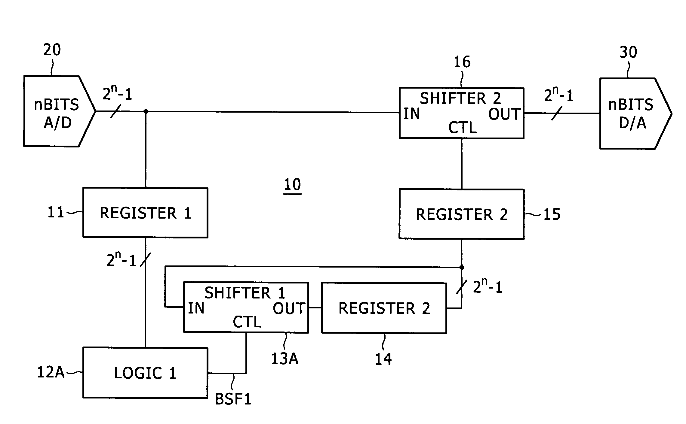
[0042]FIG. 5 shows a typical structure of a linearity enhancement circuit 10 of a D / A converter implemented as the first embodiment of the present invention adopting the DWA scheme. The linearity enhancement circuit 10 as the first embodiment has an n-bit A / D converter 20 disposed on the input side and an n-bit D / A converter 30 on the output side.

[0043]FIG. 5 shows a case in which the n-bit A / D converter 20 is used. The output of the n-bit A / D converter 20 is illustratively the thermometer code of (2n−1) bits. For example, the output of a three-bit A / D converter is seven bits. The thermometer code is a code representing values by the number of “1” bits.

[0044]The linearity enhancement circuit 10 is structured to include a first register 11, a first logic block 12 acting as a first shift amount creation block, a first shifter circuit 13, a second register 14, a second logic block 5 acting as a second shift amount creation block, and a second shifter circuit 16. The ...

second embodiment

2. Second Embodiment

[0073]FIG. 12 is a block diagram showing a typical structure of a linearity enhancement circuit 10A of a D / A converter implemented as the second embodiment of the present invention adopting the DWA scheme. FIG. 12 shows an example in which a three-bit A / D converter and a three-bit D / A converter are used. The linearity enhancement circuit 10A of the second embodiment is different from the linearity enhancement circuit 10 of the first embodiment in the following points.

[0074]The linearity enhancement circuit 10A of the second embodiment does not have a second logic block. The first logic block of the second embodiment does not convert the thermometer code of (2n−1) bits (i.e., 7 bits in this example) to decimal numbers. Instead, the first logic block feeds the seven-bit code to the first shifter circuit 13A. In addition to the first register 11A and second register 14A, a third register 17 is disposed in the output stage of the second shifter circuit 16A. The first...

third embodiment

3. Third Embodiment

[0129]FIG. 17 is a block diagram showing a typical structure of a ΣΔ A / D converter 100 implemented as the third embodiment of the present invention. The ΣΔ A / D converter 100 is made up of a filter block 110, an n-bit A / D converter 120 of low resolution (e.g., 1 to 5 bits), a D / A converter 130 having the same number of bits as the A / D converter, a linearity enhancement circuit 140, and a subtractor 150 in the input stage. Being a feedback-based system, the ΣΔ A / D converter 100 reduces the nonlinearity and noise of the circuit and thereby provides high resolution.

[0130]The A / D converter 120 corresponds to the A / D converter 20 in FIGS. 5 and 12, and the D / A converter 130 corresponds to the D / A converter 30 also in FIGS. 5 and 12. In a feedback loop FDB, the linearity enhancement circuit 10 or 10A in FIG. 5 or 12 is adopted as the linearity enhancement circuit 140 connected interposingly between the output of the A / D converter 120 and the input of the D / A converter 13...


PUM


Abstract

A linearity enhancement circuit is disclosed which includes: a first shift amount creation block creating a first shift amount in keeping with the immediately preceding output code of an n-bit A / D converter; a first shifter circuit bit-shifting input code data by the first shift amount that has been supplied, the first shifter circuit further outputting the bit-shifted input code data; a register storing the output of the first shifter circuit in order to output the stored data as the input code data to the first shifter circuit thereby forming a loop circuit in conjunction with the first shifter circuit, the register further outputting the stored code data as a second shift amount; and a second shifter circuit bit-shifting the output code of the A / D converter by the second shift amount that has been supplied, the second shifter circuit further outputting the bit-shifted output code to an n-bit D / A converter.

Description

BACKGROUND OF THE INVENTION[0001]1. Field of the Invention[0002]The present invention relates to a linearity enhancement circuit of a digital / analog (D / A) converter, a ΣΔ A / D converter, and a reception apparatus. More particularly, the invention relates to a linearity enhancement circuit used by an A / D converter and a D / A converter involving the use of ΣΔ modulation, such as a feedback D / A converter inside a ΣΔ A / D converter and a ΣΔ D / A converter.[0003]2. Description of the Related Art[0004]FIG. 1 is a block diagram showing a basic structure of a ΣΔ A / D converter. The ΣΔ A / D converter 1 is made up of a filter block 2, an A / D converter 3 with low resolution (of 1 to 5 bits), a D / A converter 4 having the same bit count as the A / D converter 3, and a subtractor 5 at the input stage. Because the ΣΔ A / D converter is a feedback-based system, the nonlinearity and noise of the circuit are reduced and high resolution is implemented thereby.[0005]However, the closer the components of the ΣΔ A...

Claims


Application Information

Patent Timeline
Patent Type & Authority Patents(United States)
IPC IPC(8): H03M1/12
CPCH03M1/0668H03M3/464H03M1/66
Inventor MATSUMOTO, TOMOHIRO
Owner SONY CORP
Why Eureka
Try Eureka