Semiconductor device having load resistor and method of fabricating the same

a technology of load resistor and semiconductor device, which is applied in the direction of semiconductor device, diode, electrical apparatus, etc., can solve the problem of not being able to use floating gate polysilicon layer as a resistor devi

Inactive Publication Date: 2007-12-11
SAMSUNG ELECTRONICS CO LTD
View PDF7 Cites 7 Cited by
  • Summary
  • Abstract
  • Description
  • Claims
  • Application Information

AI Technical Summary

Benefits of technology

[0017]Other embodiments of the invention include a method of fabricating the above-described semiconductor device and the above-described nonvolatile memory device. According to some embodiments, a nonvolatile memory device may be fabricated to prevent contact failures of resistor devices while still making use of a SAP process.

Problems solved by technology

As a result, when a resistor device is required on the isolation layer, it is not possible to use the floating gate polysilicon layer as a resistor device.

Method used


Image

  • Semiconductor device having load resistor and method of fabricating the same
  • Semiconductor device having load resistor and method of fabricating the same
  • Semiconductor device having load resistor and method of fabricating the same

Examples


Embodiment Construction

[0027]The principles of the invention will now be described more fully hereinafter with reference to the accompanying drawings, in which exemplary embodiments of the invention are shown. This invention may, however, be embodied in different forms and should not be construed as limited to the embodiments set forth herein. Rather, these embodiments are provided so that this disclosure is thorough and complete and fully conveys the scope of the invention to those skilled in the art. In the drawings, the thicknesses of layers and regions are exaggerated for clarity. The same reference numerals are used to denote the same elements.

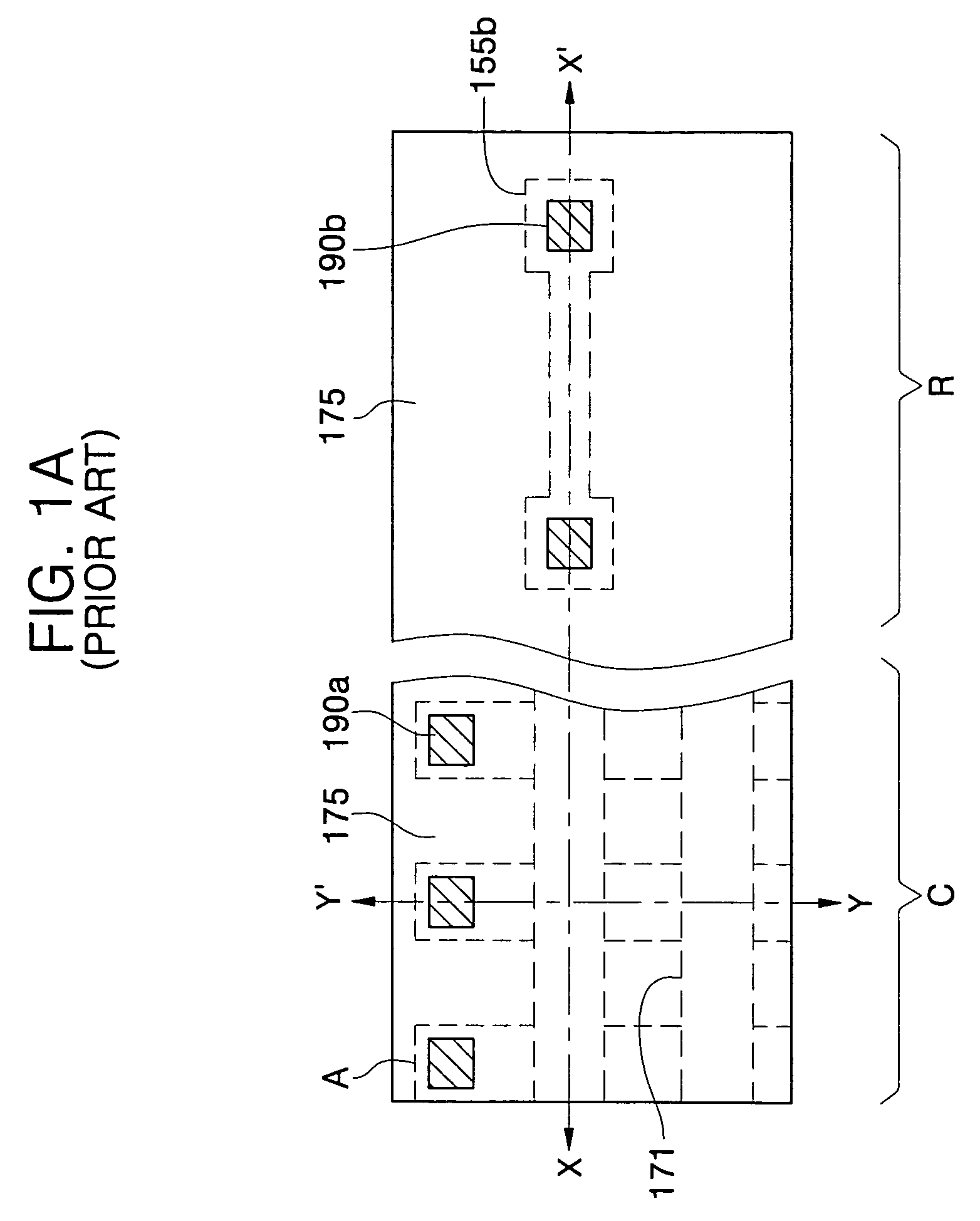
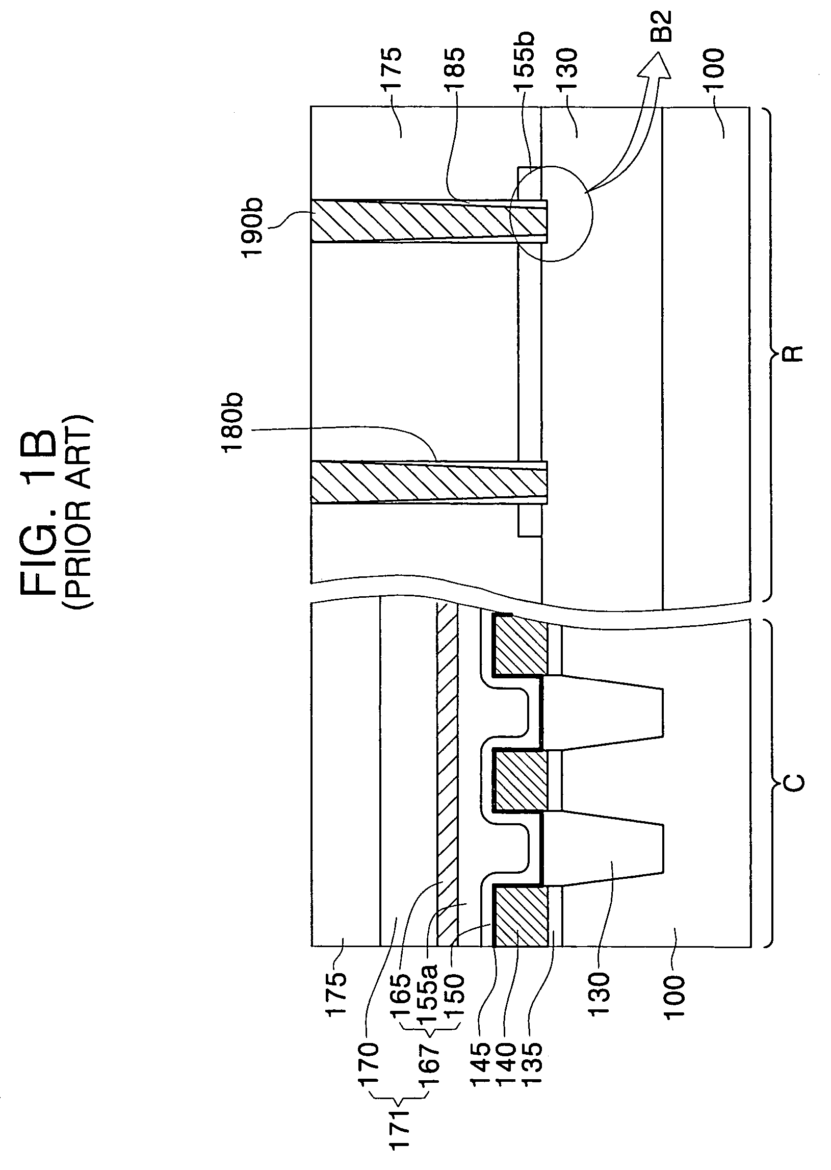
[0028]Although the exemplary embodiments described below illustrate a nonvolatile memory device, the principles of the invention may be applied to all semiconductor devices that are fabricated using SAP process.

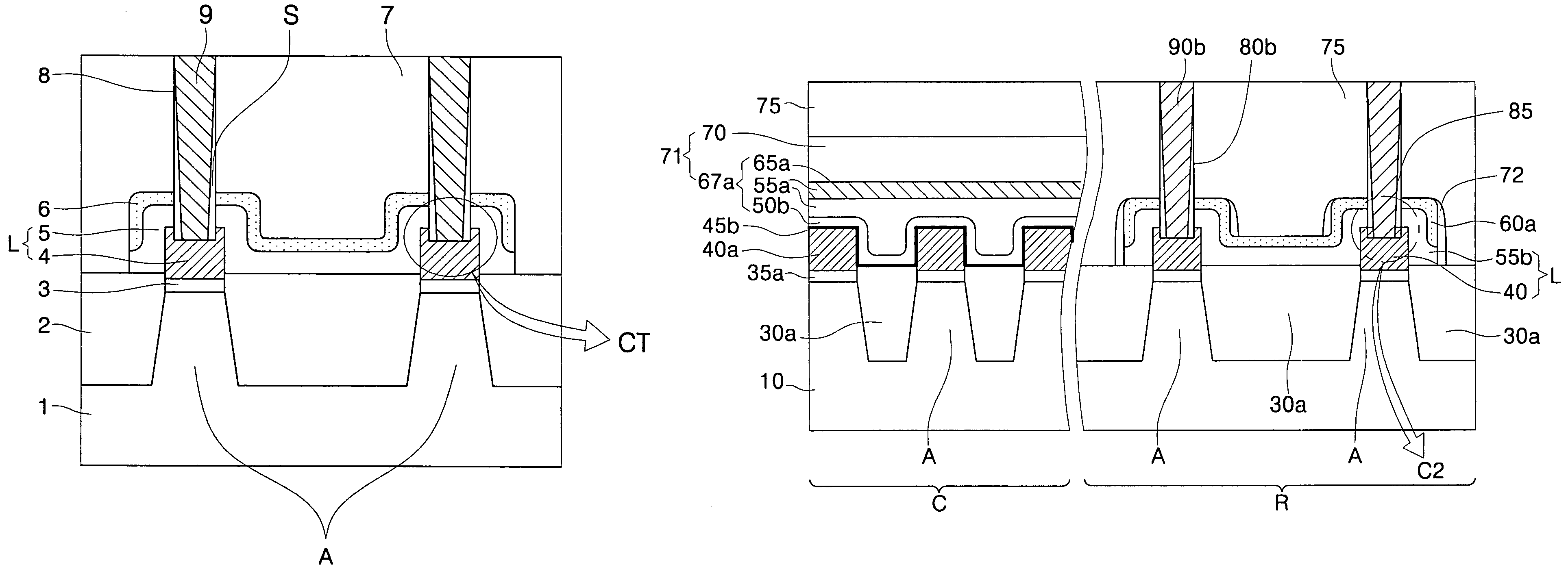
[0029]FIG. 2A is a plan diagram illustrating a nonvolatile memory device according to some embodiments of the invention. FIG. 2B is a sectional diagram ...


PUM


Abstract

A semiconductor device includes a semiconductor substrate having a resistor region, an isolation layer disposed in the resistor region, the isolation layer defining active regions, first conductive layer patterns disposed on the active regions, a second conductive layer pattern covering the first conductive layer patterns and disposed on the isolation layer, the second conductive layer pattern and the first conductive layer patterns constituting a load resistor pattern, an upper insulating layer disposed over the load resistor pattern, and resistor contact plugs disposed over the active regions, the resistor contact plugs penetrating the upper insulating layer to contact the load resistor pattern.

Description

CROSS-REFERENCE TO RELATED APPLICATIONS[0001]This application claims priority from Korean Patent Application No. 10-2004-0101345, which was filed on 3 Dec. 2004, and claims priority from Korean Patent Application No. 10-2005-0028653, which was filed on 6 Apr. 2005. The disclosures of the Korean Patent Applications identified above are incorporated by reference in their entirety.BACKGROUND[0002]1. Field of the Invention[0003]This disclosure relates to semiconductor devices and more particularly, to a semiconductor device having a load resistor and a method of fabricating the same.[0004]2. Description of the Related Art[0005]In recent years, semiconductor devices such as nonvolatile memory devices have been widely used in electronic products like computers and digital cameras. Nonvolatile memory devices are memory devices that can electrically erase or program data. A memory cell of the nonvolatile memory device typically has a floating gate, which is used as a charge storage layer, a...

Claims


Application Information

Patent Timeline
Patent Type & Authority Patents(United States)
IPC IPC(8): H01L21/20
CPCH01L27/0629H01L27/11531H01L27/11526H01L27/105H10B41/42H10B41/40
Inventor CHOI, EUN-YOUNGBAEK, EUN-JIN
Owner SAMSUNG ELECTRONICS CO LTD
Why Eureka
Try Eureka