Wafer holder, heater unit having the wafer holder, and wafer prober having the heater unit

a heater unit and wafer technology, applied in the direction of instruments, basic electric elements, measurement devices, etc., can solve the problems of long time between the increase and decrease temperature of the heater, the contact failure between the wafer and the probe pin, and the improvement of the throughput, so as to effectively prevent the contact failure and improve the heat-insulating effect, the effect of less susceptible to deformation

Inactive Publication Date: 2007-04-12
SUMITOMO ELECTRIC IND LTD
View PDF3 Cites 6 Cited by
  • Summary
  • Abstract
  • Description
  • Claims
  • Application Information

AI Technical Summary

Benefits of technology

[0010] The present invention was made to solve the above-described problems. Specifically, an object of the present invention is to provide a wafer holder less susceptible to deformation even under high load and hence capable of effectively preventing contact failure, a

Problems solved by technology

Therefore, when the chuck top is thin, the chuck top might possibly be deformed, resulting in contact failure between the wafer and a probe pin.
As a result, it takes long time to increase and decrease temperature of the heater, which is a significant drawback in improving the throughput.
As recent chips come to have higher outputs, it is possible that a chip generates considerable heat during measurement of electric characteristics, and in some situations, the chip might be broken by self-heating.
Therefore, when the wafer prober is supported only by the outermost circumference as described in Japanese Patent Laying-Open No. 2001-033484, the prober itself may deform because of the load at the time of probing, uniform contact of the pins of probe card with the wafe

Method used


Image

  • Wafer holder, heater unit having the wafer holder, and wafer prober having the heater unit
  • Wafer holder, heater unit having the wafer holder, and wafer prober having the heater unit
  • Wafer holder, heater unit having the wafer holder, and wafer prober having the heater unit

Examples


example 1a

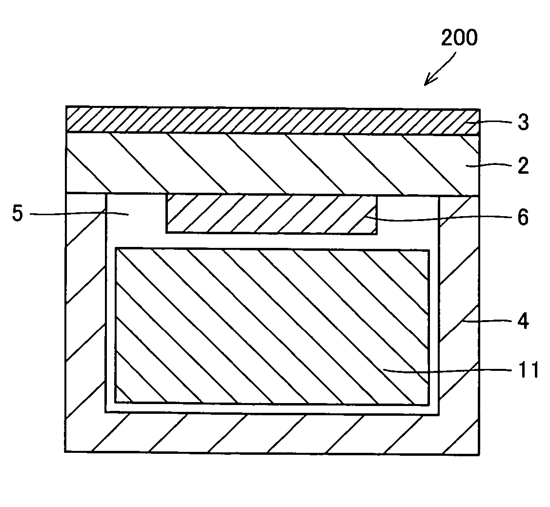
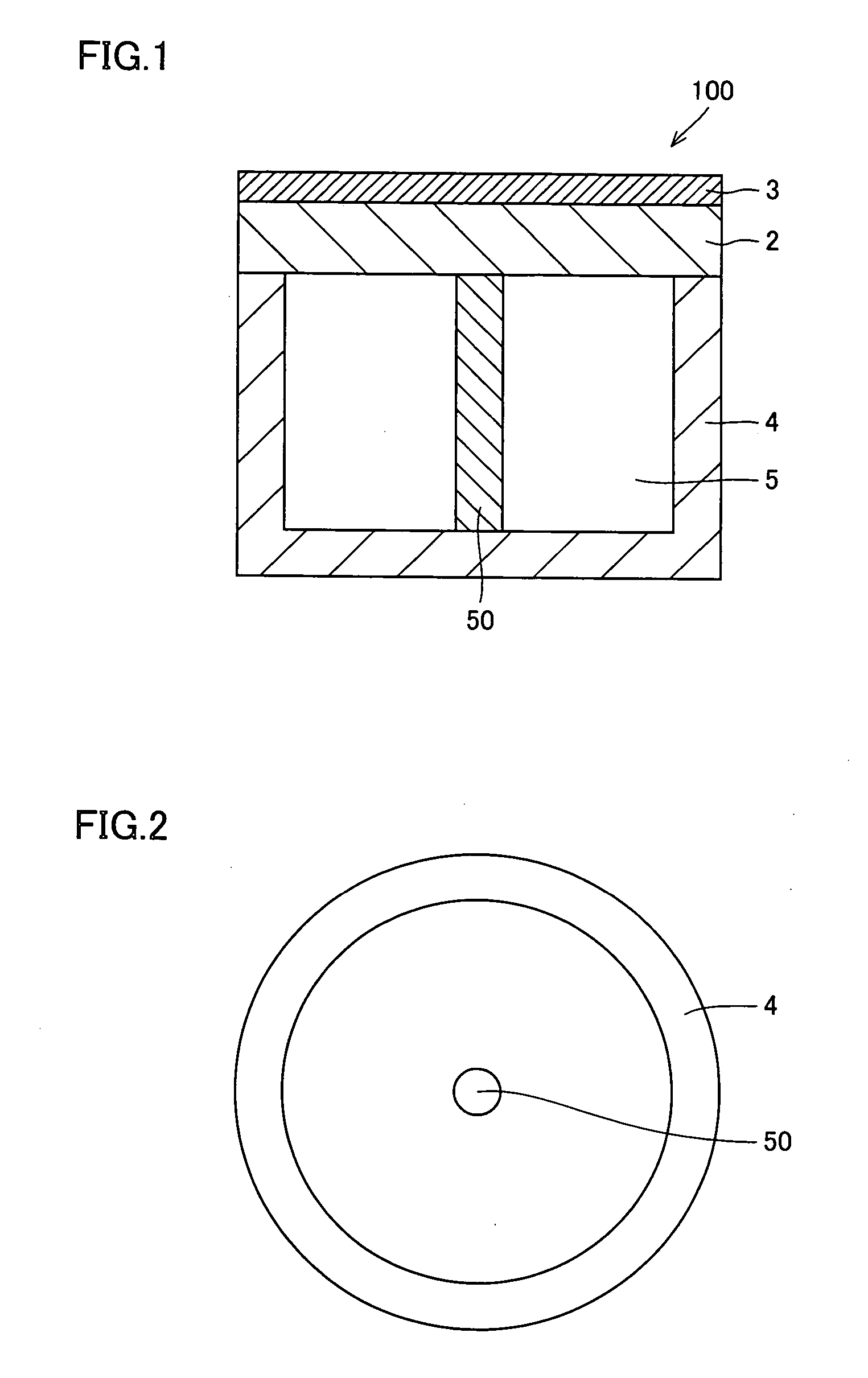
[0118] Wafer holder 100 shown in FIG. 1 was fabricated. An Si—SiC substrate having the diameter of 310 mm and the thickness of 15 mm was prepared. On one surface of the substrate, a concentric trench and through holes for vacuum chucking a wafer were formed, and nickel plating was applied as the chuck top conductive layer 3, to provide a wafer-mounting surface. Thereafter, the wafer-mounting surface was polished and finished to have the overall warp amount of 10 μm and the surface roughness Ra of 0.02 μm, and chuck top 2 was completed.

[0119] Thereafter, a mullite-alumina composite body of a pillar shape having the diameter of 310 mm and thickness of 40 mm was prepared as supporter 4. The surface of supporter 4 in contact with the chuck top and the bottom surface are finished to the flatness of 0.09 mm, and the surface on the side of chuck top 2 was counter-bored to have the inner diameter of 290 mm and the depth of 20 mm, to provide the space for mounting heater body 6 shown in FIG...


PUM


Abstract

A wafer holder less susceptible to deformation even under high load and having high heat-insulating effect and hence capable of improving positional accuracy, improving thermal uniformity and rapid heating and cooling of chips, as well as a heater unit including the wafer holder and a wafer prober including the heater unit are provided. The wafer holder includes a chuck top having a chuck top conductive layer on its surface and a supporter supporting the chuck top, and has a support member in a space between the chuck top and the supporter. Preferably, the support member is arranged concentric with the supporter or approximately at the center of the supporter, and more preferably, support members arranged concentrically and arranged at the center are both provided.

Description

BACKGROUND OF THE INVENTION [0001] 1. Field of the Invention [0002] The present invention relates to a wafer holder used for a wafer prober in which a semiconductor wafer is mounted on a wafer-mounting surface and a probe card is pressed onto the wafer for inspecting electric characteristics of the wafer, a heater unit including the wafer holder and to a wafer prober including the heater unit. [0003] 2. Description of the Background Art [0004] Conventionally, in the step of inspecting a semiconductor, a semiconductor substrate (wafer) as an object of processing is subjected to heat treatment. Specifically, burn-in is performed in which the wafer is heated to a temperature higher than the temperature of normal use, to accelerate degradation of a possibly defective semiconductor chip and to remove the defective chip, in order to prevent defects after shipment. In the burn-in process, after semiconductor circuits are formed on the semiconductor wafer and before cutting the wafer into i...

Claims


Application Information

Patent Timeline
IPC IPC(8): F24J3/00
CPCG01R31/2863G01R31/2875H01L21/68757
Inventor ITAKURA, KATSUHIRONATSUHARA, MASUHIRONAKATA, HIROHIKOAWAZU, TOMOYUKINISHI, TERUTO
Owner SUMITOMO ELECTRIC IND LTD
Why Eureka
Try Eureka