
Distortion compensating and power amplifying apparatus

a technology of distortion compensation and power amplifier, applied in the direction of dynamo-electric components, amplifier modifications to reduce non-linear distortion, transmission, etc., can solve the problem that the distortion compensation becomes ineffective for the power amplifier at given power, and achieve the effect of reducing improving the distortion compensation effect, and high output power

Inactive Publication Date: 2007-12-11
SONY MOBILE COMM INC
View PDF4 Cites 16 Cited by
  • Summary
  • Abstract
  • Description
  • Claims
  • Application Information

AI Technical Summary

Benefits of technology

The solution enhances distortion compensation effectiveness for higher output powers, increasing the inflection point power and improving the adjacent channel power ratio, thereby reducing distortion and power consumption in cellular phone terminals.

Problems solved by technology

That is, the distortion compensation becomes ineffective for the power amplifier at given power.

Method used


Image

  • Distortion compensating and power amplifying apparatus
  • Distortion compensating and power amplifying apparatus
  • Distortion compensating and power amplifying apparatus

Examples


second embodiment

[0072]FIG. 9 is a block diagram showing the present invention. The mutually corresponding parts in FIGS. 9 and 1 are designated by the same reference numerals. There are following differences from the apparatus in FIG. 1. The phase circuit 15 in FIG. 1 is removed and a matching circuit 25 is inserted instead. The matching circuit 11 preceding the FET 12 is changed to a matching circuit 21. The inventors already proposed such construction in JP-B No. 32351 / 2004.

[0073]Operations of the apparatus in FIG. 9 are described below. When an input signal is input to an input terminal IN, the branch circuit 10 branches the input signal into two signals. One of the branched signals passes through the matching circuit 21 and is input to the source-grounded FET 12. The band pass filter 13 extracts a second harmonic generated in the FET 12. The attenuation circuit 14 adjusts the second harmonic's amplitude. The signal passes through the second matching circuit 25 and is input to a first input term...

third embodiment

[0077]FIG. 12 is a block diagram showing the present invention. The mutually corresponding parts in FIG. 12 and the above-mentioned embodiments are designated by the same reference numerals.

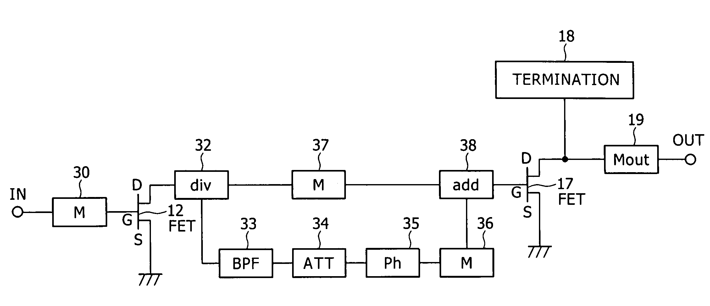
[0078]The power amplifying apparatus includes two stages of amplifiers, i.e., a first source-grounded FET 12 and a second source-grounded FET 39 directly connected to each other. The amplifying apparatus further includes a first matching circuit 30, a branch circuit 32, a second matching circuit 37, a band pass filter 33, an attenuation circuit 34, a phase circuit 35, a third matching circuit 36, an addition circuit 38, a second harmonic termination circuit 18, and a matching circuit 19. The first matching circuit 30 is connected between an input terminal IN and the gate of the first FET 12. The branch circuit 32 is connected to a drain terminal of the source-grounded FET 12 to branch drain output into two signals. The second matching circuit 37 is connected between a second output terminal of th...


PUM


Abstract

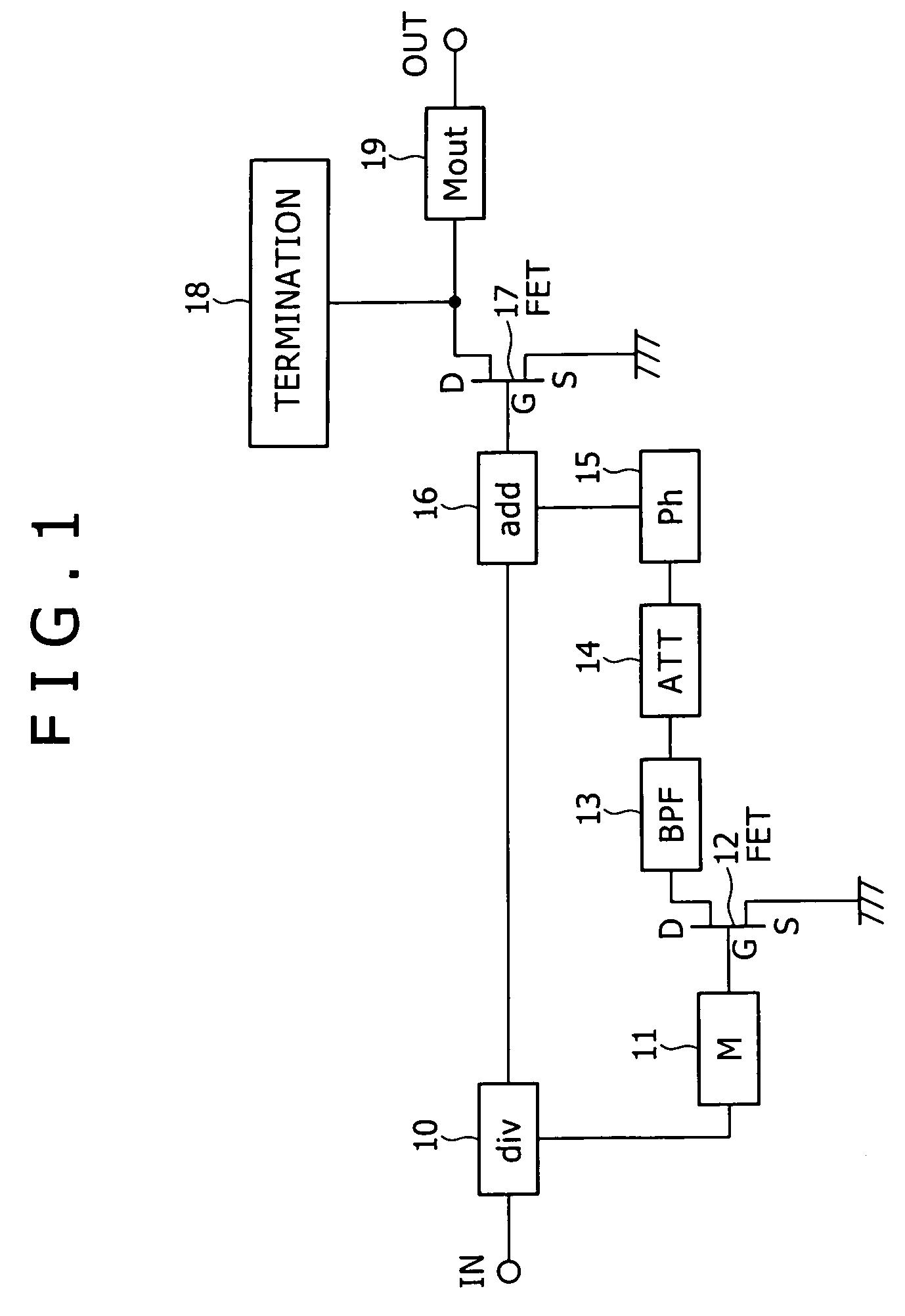
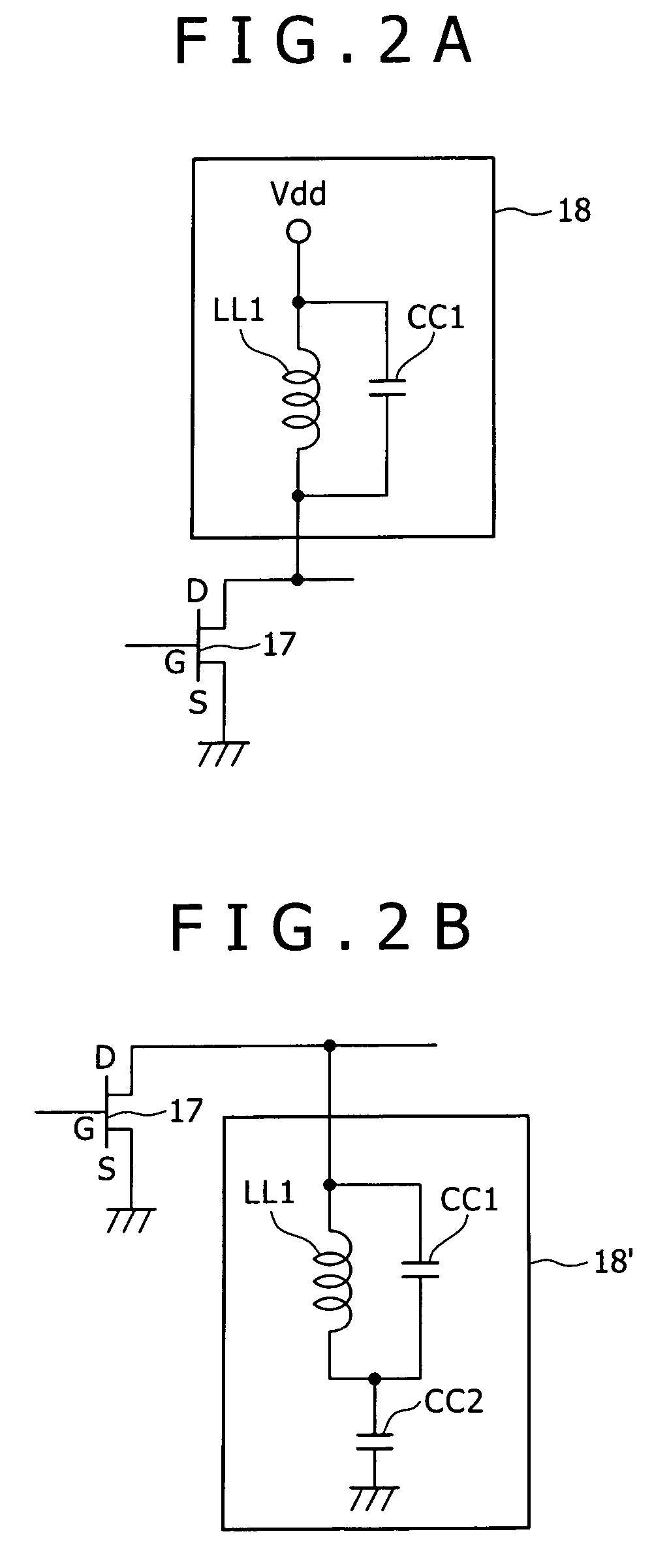
Disclosed is a distortion compensating and power amplifying apparatus including: a transistor to power amplifies an input signal; a branch circuit to branch the input signal into two signals; distortion compensation means for generating a second harmonic of a fundamental wave for one of branched signals and adding the generated second harmonic to the other branch signal from said branch circuit for input to an input terminal of said transistor; and a termination circuit connected to an output terminal of said transistor and grounding the second harmonic.

Description

CROSS REFERENCES TO RELATED APPLICATIONS[0001]The present invention contains subject matter related to Japanese Patent Application JP 2004-135363 filed in the Japanese Patent Office on Apr. 30, 2004, the entire contents of which being incorporated herein by reference.BACKGROUND OF THE INVENTION[0002]1. Field of the Invention[0003]The present invention relates to a distortion compensating apparatus and particularly to a distortion compensating apparatus applicable to high-frequency power amplifiers for cellular phones.[0004]2. Description of Related Art[0005]In the past, a cellular phone using the CDMA (Code Division Multiple Access) system always varies terminal's transmission power. The output distribution often peaks approximately 10 mW when the speech communication is used. In many cases, a CDMA cellular phone terminal uses a DC-DC converter to vary power supply voltages of a power amplifier (PA) at low and high outputs so that the efficiency for low outputs is improved. The long...

Claims


Application Information

Patent Timeline
Patent Type & Authority Patents(United States)
IPC IPC(8): H03F1/26H03F1/32H03F3/24H04B1/04
CPCH03F1/3223H03F1/3205H02K15/165
Inventor KUSUNOKI, SHIGEOHATSUGAI, TADANAGA
Owner SONY MOBILE COMM INC
Learn More