Semiconductor package having heat spreader and package stack using the same

a technology of semiconductor devices and heat spreaders, applied in semiconductor devices, semiconductor/solid-state device details, constructions, etc., can solve problems such as degeneration of performance, electromagnetic interference (emi), and inability to improve electrical performance, so as to improve the protection from emi and improve the effect of emi protection

Active Publication Date: 2008-01-08
SAMSUNG ELECTRONICS CO LTD
View PDF20 Cites 30 Cited by
  • Summary
  • Abstract
  • Description
  • Claims
  • Application Information

AI Technical Summary

Benefits of technology

[0012]A semiconductor package with a heat shield is provided that does not require additional means to electrically connect upper and lower packages and provides improved protection from electromagnetic interference.
[0013]One embodiment provides a chip mounted on a board with a heat spreader mounted on a rear side of the chip. External contact terminals protrude a height greater than the combined height of the chip and heat spreader from the lower surface of the board. Ground bumps can connect the board to the heat spreader for improved protection from EMI.
[0015]Yet another embodiment provides a chip mounted on an upper surface of a board with a heat spreader mounted on a lower surface of the board. External contact terminals protrude a height greater than the combined height of the chip and heat spreader from the lower surface of the board. A predetermined number of external contact terminals protrude through and connect with ground holes in the heat spreader. The remaining external contact terminals are vertically exposed by the heat spreader. A top heat spreader can be attached to the rear side of the chip and ground bumps can connect contact pads on the upper surface of the board to the top heat spreader for improved protection from EMI.
[0016]Yet another embodiment stacks the packages with heat spreaders mounted on the lower surfaces of the board. The external contact terminals of an upper package are connected with contact pads located on the upper surface of the board in the lower package. A top heat spreader can be attached to the rear side of the chip in the upper package and ground bumps can connect contact pads on the upper surface of the board in the upper package to the top heat spreader for improved protection from EMI.

Problems solved by technology

A semiconductor package suitable for high speed and performance generates a large quantity of heat during the operation, which results in degeneration of performance.
However, since the heat spreaders in the prior art have a structure where a thermal conductive pad is simply attached on the rear side of a molding body or a semiconductor chip, the prior art merely improved heat dissipation while not improving electrical performance.
This kind of structure in the prior art can even cause electromagnetic interference (EMI) problems.
However, the semiconductor package having grounded a heat spreader is not suitable for a package stack within the structure disclosed in the prior art.
Those structures need additional means for electric connection between a lower package and an upper package because the upper package is placed on the heat spreader of the lower package, which results in increasing the thickness or width of the package stack.

Method used


Image

  • Semiconductor package having heat spreader and package stack using the same
  • Semiconductor package having heat spreader and package stack using the same
  • Semiconductor package having heat spreader and package stack using the same

Examples


first exemplary embodiment

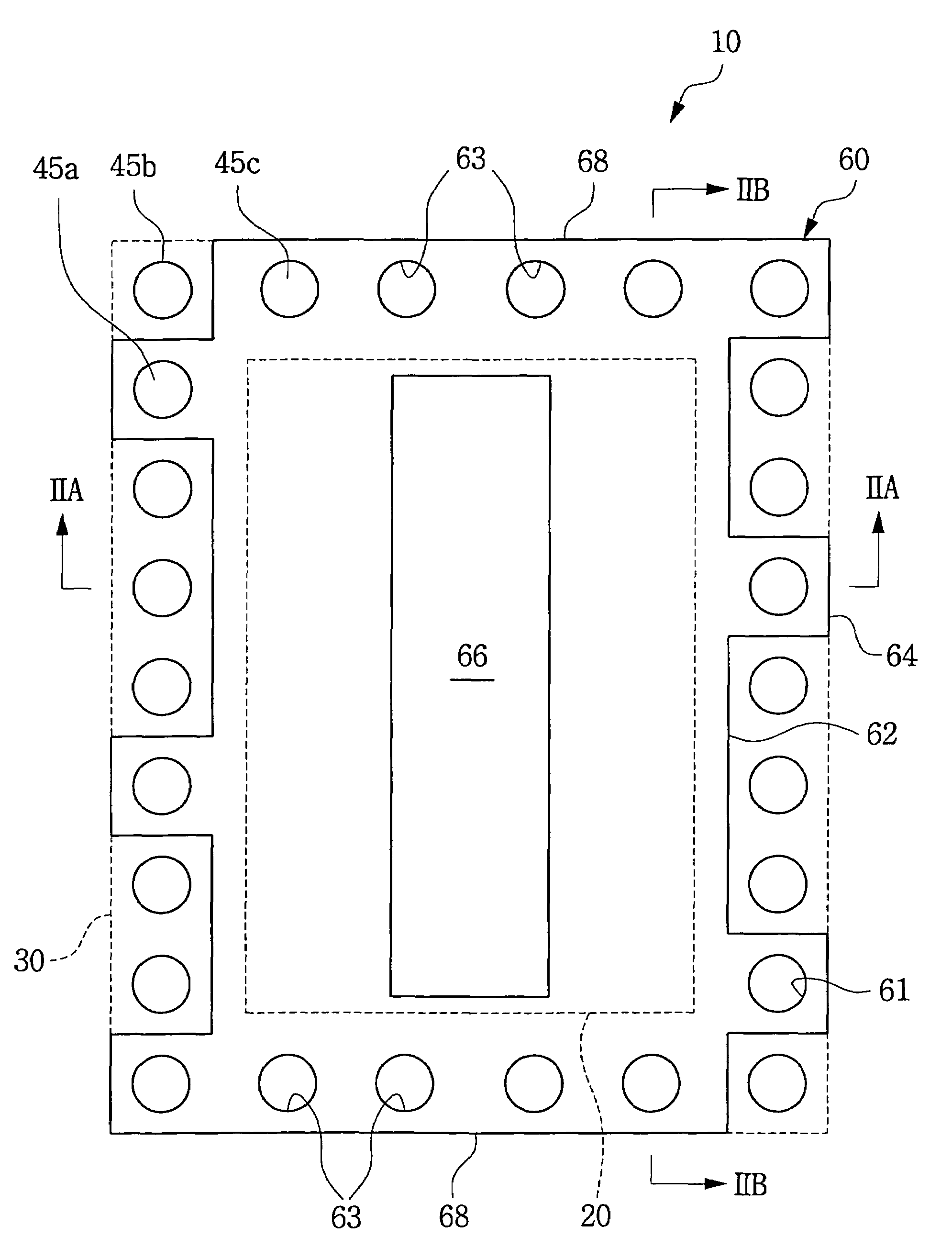
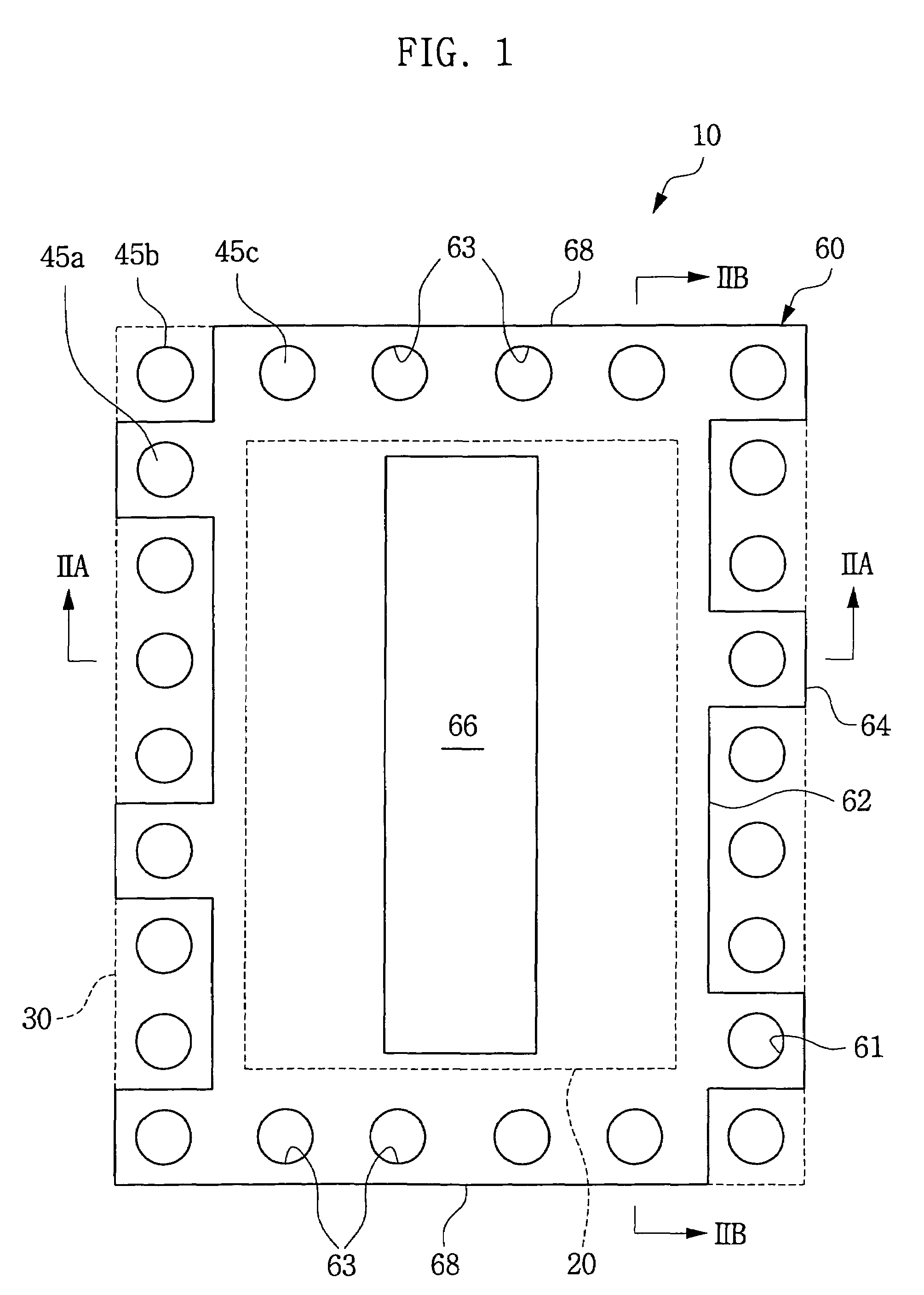
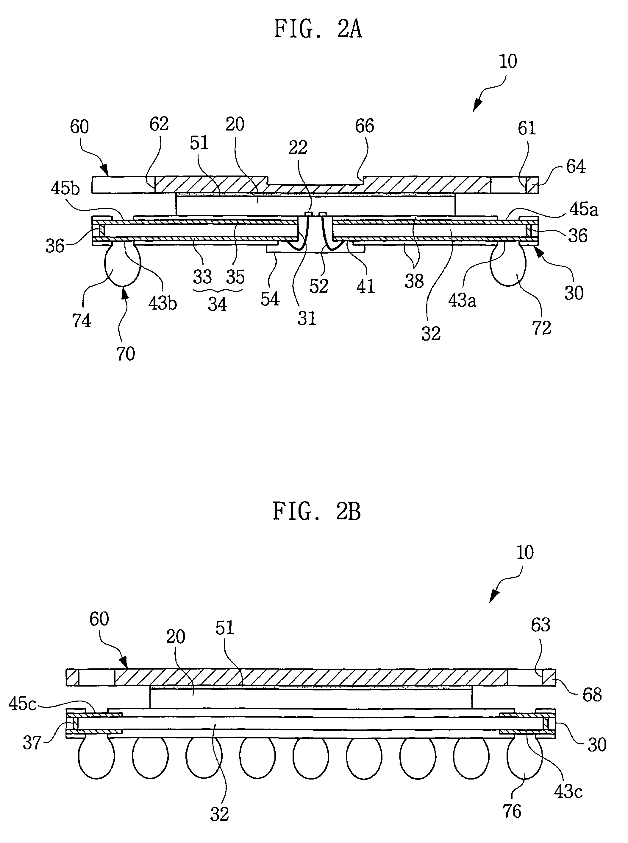
[0039]FIG. 1 is a plan view of a semiconductor package having heat spreader according to a first exemplary embodiment of the present invention. FIG. 2A is a cross-sectional view taken along the line IIA-IIA in FIG. 1. FIG. 2B is a cross-sectional view taken along the line IIB-IIB in FIG. 1.

[0040]Referring to FIGS. 1 through 2B, in the semiconductor package 10, according to the first exemplary embodiment of the present invention, the semiconductor chip 20 is mounted on and connected with the board 30 with its active surface facing the upper surface of the board 30. The heat spreader 60 is attached to the rear side of the semiconductor chip 20. And the external terminals 70 are formed on the peripheral part of the lower surface of the board 30.

[0041]More specifically, the semiconductor chip 20 is a center pad type, of which bonding pads 22 are formed on the center region of the active surface. Generally, a center pad type semiconductor chip is more favorable for high-speed operation t...


PUM


Abstract

A semiconductor package which can be stacked to form a package stack that includes a semiconductor chip with bonding pads, a board having contact pads on its upper surface and bump pads on its lower surface, a heat spreader attached to the rear side of the semiconductor chip and covering the upper surface of the board, and external contact terminals including ground terminals and signal terminals formed on the bump pads. The contact pads of the board include ground contact pads connected with the ground terminals and signal contact pads connected with the signal terminals. The heat spreader includes indented parts to expose the signal contact pads and protruded parts to cover the ground contact pads which are exposed through holes formed on the protruded parts on the peripheral part of the heat spreader. The semiconductor package can alternatively have the heat spreader attached to the lower surface of the board.

Description

CROSS REFERENCE TO RELATED APPLICATIONS[0001]This U.S. non-provisional application claims priority under 35 U.S.C. §119 to Korean Patent Application No. 2004-16179 filed Mar. 10, 2004, the contents of which are incorporated herein in its entirety by reference.BACKGROUND OF THE INVENTION[0002]1. Field of the Invention[0003]The present invention relates generally to a semiconductor package and a package stack using the same and, more particularly, to a semiconductor package having a heat spreader and a package stack using the same.[0004]2. Description of the Related Art[0005]The electronics industry continues to seek products that are lighter, faster, smaller, multi-functional, more reliable and more cost-effective. One of the important technologies making these objectives possible is semiconductor packaging technology by which a chip scale package (CSP) was recently realized. CSP technology provides a small sized package having the size level of a semiconductor chip.[0006]A semicondu...

Claims


Application Information

Patent Timeline
Patent Type & Authority Patents(United States)
IPC IPC(8): H01L23/02H01L23/34H01L23/36
CPCH01L23/3157H01L23/552H01L25/105H01L23/13H01L2924/07802H01L2924/15151H01L2225/1088H01L2224/73253H01L2224/73215H01L2224/32225H01L2924/3025H01L2924/15331H01L2924/01079H01L2225/1094H01L2225/1058H01L24/16H01L24/29H01L24/32H01L24/48H01L24/73H01L2224/16225H01L2224/291H01L2224/2919H01L2224/32245H01L2224/48091H01L2224/4824H01L2224/73204H01L2224/73265H01L2225/1023H01L2924/00014H01L2924/00H01L2224/05026H01L2224/05573H01L2224/05599H01L2224/45099H01L2924/00012H01L2224/45015H01L2924/207E01H1/005
Inventor LEE, JONG-JOOSONG, YOUNG-HEE
Owner SAMSUNG ELECTRONICS CO LTD
Why Eureka
Try Eureka