Electrical interconnection structure formation

a technology of electrical interconnection and structure, applied in the direction of electrical apparatus, semiconductor devices, semiconductor/solid-state device details, etc., can solve the problem that the electrical structure connected to another electrical structure may not constitute a structurally adequate connection

Active Publication Date: 2008-01-29
AURIGA INNOVATIONS INC
View PDF20 Cites 61 Cited by
  • Summary
  • Abstract
  • Description
  • Claims
  • Application Information

AI Technical Summary

Problems solved by technology

An electrical structure connected to another electrical structure may not comprise a structurally adequate connection.

Method used


Image

  • Electrical interconnection structure formation
  • Electrical interconnection structure formation
  • Electrical interconnection structure formation

Examples


Embodiment Construction

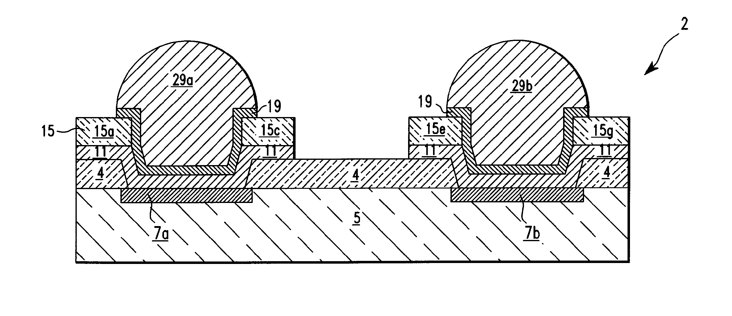
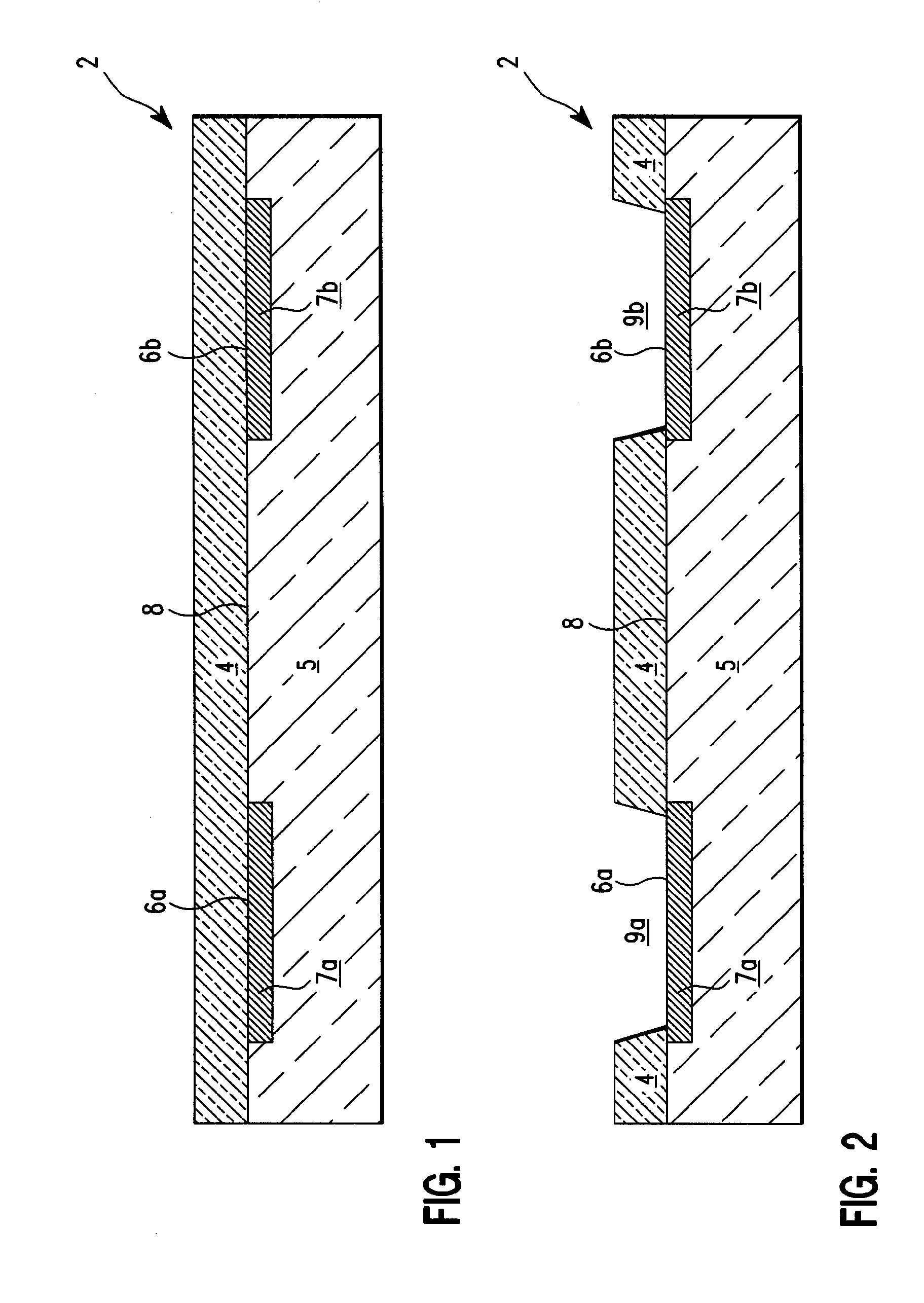
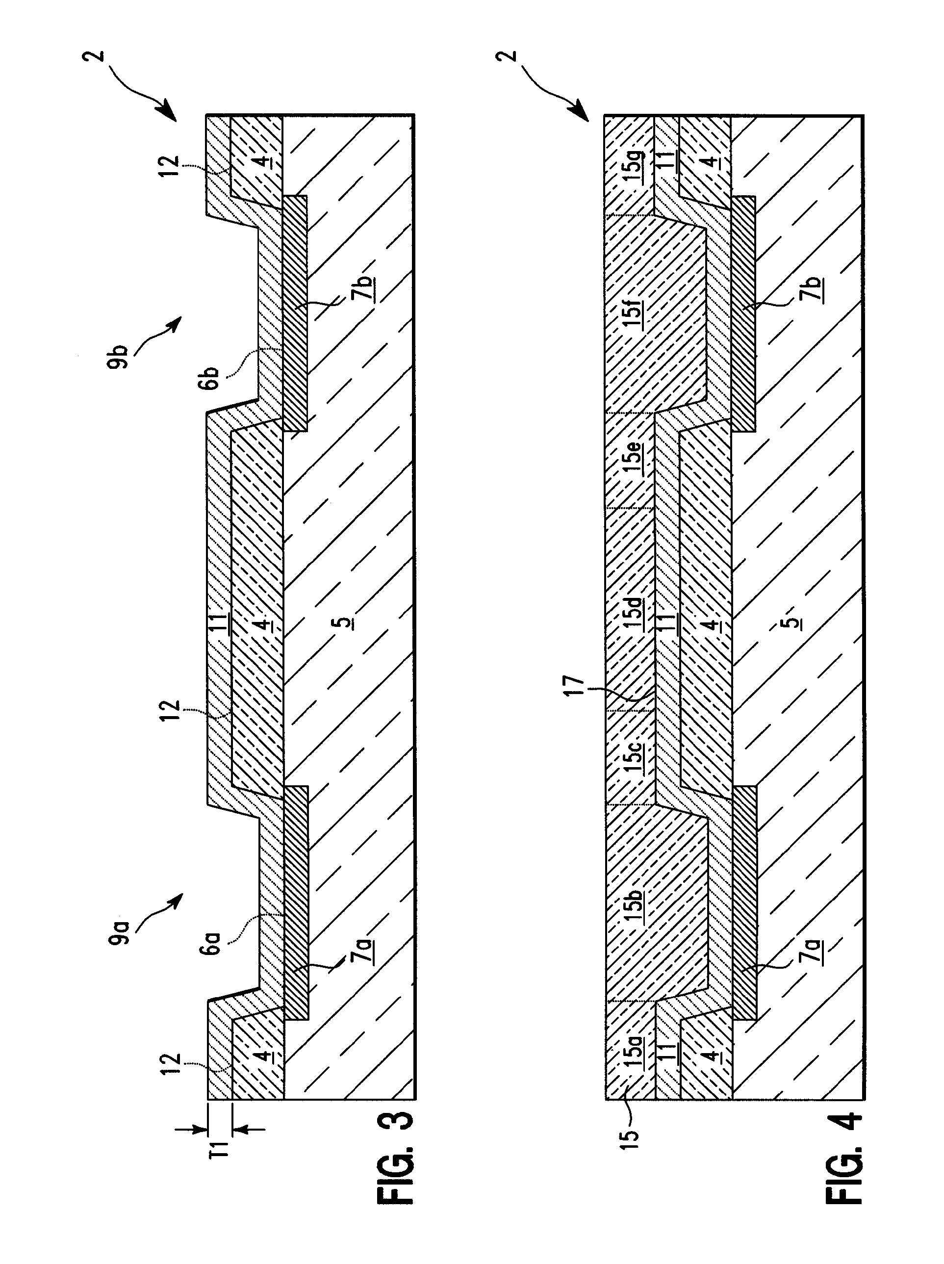
[0039]FIGS. 1-12 illustrate and describe stages in a fabrication process of an electrical (interconnection) structure 2, in accordance with embodiments of the present invention. The electrical structure 2 illustrated in FIGS. 1-12 is a cross sectional view. The electrical structure 2 may comprise any electrical structure known to a person of ordinary skill in the art including, inter alia, a semiconductor device, etc. The fabrication process described with respect to FIGS. 1-12 comprises the formation of a connecting means (e.g., see solder balls 29a and 29b in FIG. 12) for electrically and mechanically connecting the electrical structure 2 to another electrical structure (not shown). The fabricated electrical structure 2 illustrated in FIG. 12 may comprise, inter alia, a copper back end of the line controlled collapse chip connection (CuBEOL C4) electrical structure.

[0040]In FIG. 1, the electrical structure 2 is provided for the fabrication process, in accordance with embodiments o...


PUM

PropertyMeasurementUnit
thicknessaaaaaaaaaa
thickness T1aaaaaaaaaa
thickness T2aaaaaaaaaa

Abstract

An electrical interconnection structure and method for forming. The electrical structure comprises a substrate comprising electrically conductive pads and a first dielectric layer over the substrate and the electrically conductive pads. The first dielectric layer comprises vias. A metallic layer is formed over the first dielectric layer and within the vias. A second dielectric layer is formed over the metallic layer. A ball limiting metallization layer is formed within the vias. A photoresist layer is formed over a surface of the ball limiting metallization layer. A first solder ball is formed within a first opening in the photoresist layer and a second solder ball is formed within a second opening in the photoresist layer.

Description

BACKGROUND OF THE INVENTION[0001]1. Technical Field[0002]The present invention relates to an electrical connection structure and associated forming method.[0003]2. Related Art[0004]An electrical structure connected to another electrical structure may not comprise a structurally adequate connection. Therefore there exists a need for a means for connecting an electrical structure to another electrical structure comprising a structurally adequate connection.SUMMARY OF THE INVENTION[0005]The present invention provides a method for forming an electrical structure, comprising:[0006]providing a substrate comprising a first electrically conductive pad and a second electrically conductive pad formed within a volumetric portion of the substrate and a first dielectric layer over a surface of said substrate, a surface of said first electrically conductive pad, and a surface of said second electrically conductive pad;[0007]forming a first via and a second via in said first dielectric layer, said...

Claims


Application Information

Patent Timeline
Patent Type & Authority Patents(United States)
IPC IPC(8): H01L23/52H01L23/44
CPCH01L24/11H01L24/03H01L24/05H01L24/12H01L2924/0002H01L2224/0401H01L2224/131H01L2224/11902H01L2924/00014H01L2224/03912H01L2224/05022H01L2224/05572H01L2224/05599H01L2224/10126H01L2224/1147H01L2224/11901H01L2224/11912H01L2224/13022H01L2224/13099H01L2224/16H01L2924/01014H01L2924/01029H01L2924/01047H01L2924/0105H01L2924/01073H01L2924/01078H01L2924/01082H01L2924/014H01L2924/04953H01L2224/05027H01L2224/13007H01L2924/01006H01L2224/05018H01L2224/05558H01L2224/05552
Inventor DAUBENSPECK, TIMOTHY H.GAMBINO, JEFFREY P.MUZZY, CHRISTOPHER D.SAUTER, WOLFGANG
Owner AURIGA INNOVATIONS INC
Why Eureka
Try Eureka