ROM-based memory testing

a technology of integrated circuits and memory, applied in the direction of measurement devices, error detection/correction, instruments, etc., can solve the problems of complex integrated circuits, inconvenient testing of fabricated integrated circuits, and inability to test fabricated integrated circuits to determine proper operation

Active Publication Date: 2008-01-29
TEXAS INSTR INC
View PDF10 Cites 16 Cited by
  • Summary
  • Abstract
  • Description
  • Claims
  • Application Information

AI Technical Summary

Benefits of technology

[0009]This invention provides lots of flexibility to test memories even while doing a complete ROM-based test. This invention provides the ability to download just the algorithm information or just the memory information from the ROM.

Problems solved by technology

Testing fabricated integrated circuits to determine proper operation has always been a difficult problem.
A design defect means that the integrated circuit was manufactured to a design not proper for the intended purpose.
Such a defect will effect every integrated circuit until the design is changed.
A manufacturing defect involves some fault in the manufacture of the integrated circuit that will effect less than all parts manufactured.
With the increase in integrated circuit complexity this testing is increasingly difficult.

Method used


Image

  • ROM-based memory testing
  • ROM-based memory testing
  • ROM-based memory testing

Examples


Embodiment Construction

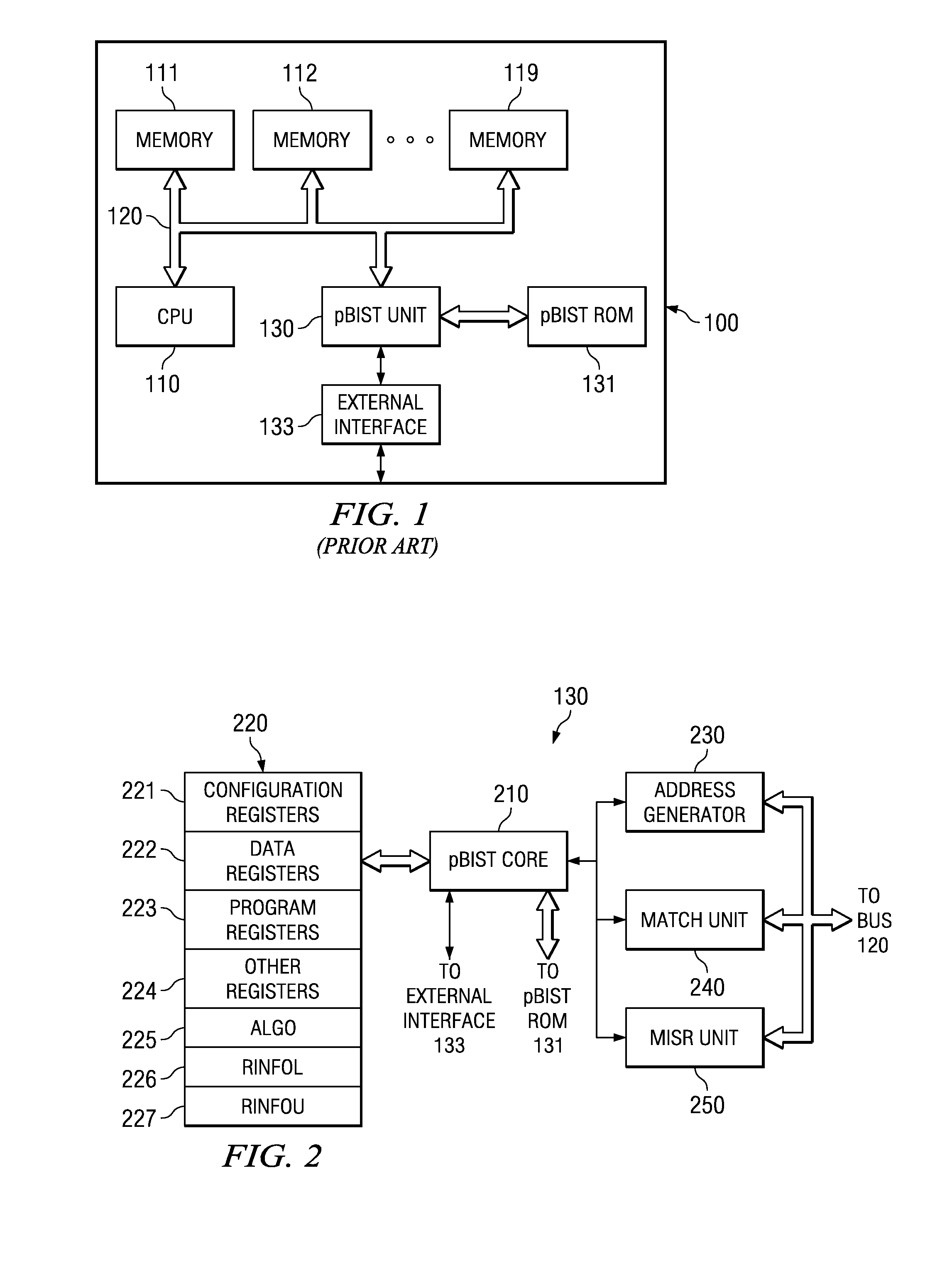
[0018]FIG. 1 illustrates a typical integrated circuit 100 including programmable built-in self test. FIG. 1 illustrates integrated circuit 100 including central processing unit (CPU) 110 and memories 111, 112 . . . 119 coupled by bus 120. These circuits are merely representative of circuits embodied in an integrated circuit including pBIST.

[0019]The programmable built-in self test includes pBIST unit 130, pBIST ROM 131 and external interface 133. pBIST unit 130 controls the tests in much the same fashion as CPU 110 controls operation of integrated circuit 100. pBIST unit 130 is controlled by test instructions stored in pBIST ROM 131. pBIST unit 130 may couple to circuits outside integrated circuit 100 via external interface 133. FIG. 1 illustrates pBIST unit 130 coupled to CPU 110 and memories 111, 112 . . . 119 via bus 120. This connection is merely illustrative of the type of connection between pBIST unit 130 and other circuits of integrated circuit 100.

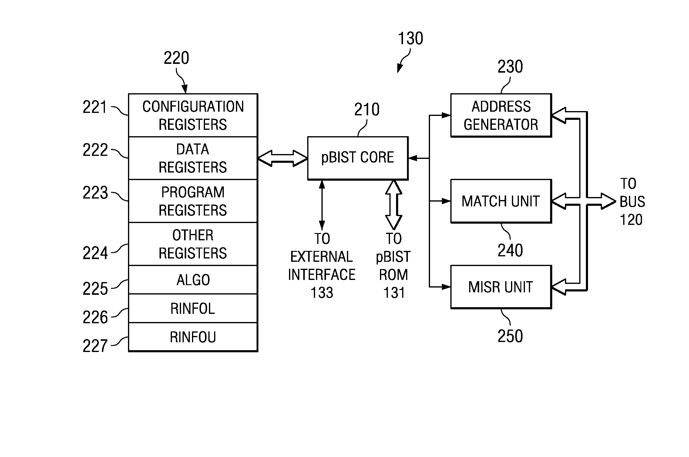
[0020]FIG. 2 illustrates a ...


PUM


Abstract

This invention uniquely partitions the pBIST ROM for storing program and data information. The pBIST unit selectively loads both the algorithm and data, the algorithm only or the data only for each test set stored in the pBIST ROM into read / write registers. These registers are memory mapped readable / writable. A configuration register has an algorithm bit and a data bit which determines whether the corresponding algorithm or data is loaded from the pBIST ROM. The pBIST unit includes another configuration register having one bit corresponding to each possible test set stored in the pBIST ROM. The pBIST unit runs a test set if the corresponding bit in the configuration register has a first digital state.

Description

CLAIM OF PRIORITY[0001]This application claims priority under 35 U.S.C. 119(e)(1) to U.S. Provisional Application No. 60 / 688,972 filed Jun. 9, 2005.TECHNICAL FIELD OF THE INVENTION[0002]The technical field of this invention is integrated circuit testing.BACKGROUND OF THE INVENTION[0003]Testing fabricated integrated circuits to determine proper operation has always been a difficult problem. There are two major types of errors. A design defect means that the integrated circuit was manufactured to a design not proper for the intended purpose. Such a defect will effect every integrated circuit until the design is changed. The integrated circuit manufacturer must detect and correct such defects before shipping large number of parts to customers to avoid a costly recall. A manufacturing defect involves some fault in the manufacture of the integrated circuit that will effect less than all parts manufactured. Such defects are corrected by identification and correction of the manufacturing f...

Claims


Application Information

Patent Timeline
Patent Type & Authority Patents(United States)
IPC IPC(8): G11C7/00G01R31/28G06F11/00G11C29/00
CPCG11C29/16G11C17/14
Inventor RAMAMURTI, ANANTHAKRISHNANDAMODARAN, RAGURAM
Owner TEXAS INSTR INC
Why Eureka
Try Eureka