CMOS image sensor with variable conversion gain

a technology of image sensor and conversion gain, which is applied in the field of cmos image sensor, can solve the problems of image overexposure, inability to reduce the exposure period below the flicker period, and the illumination level of the light source may vary over time, so as to prevent overexposure without reducing the exposure period, high conversion gain, and high light sensitivity

Active Publication Date: 2008-02-05
APTINA IMAGING CORP
View PDF3 Cites 22 Cited by
  • Summary
  • Abstract
  • Description
  • Claims
  • Application Information

AI Technical Summary

Benefits of technology

[0011]In accordance with an illustrated preferred embodiment of the present invention, a variable conversion gain pixel prevents overexposure without reducing the exposure period. Under dim lighti

Problems solved by technology

One problem associated with the rolling shutter method is that the illumination level of the light source may vary over time.
However, the exposure period cannot be reduced below the flicker period.
If the illumination is very bright, and the exposure period cannot be reduced, then the image will be o

Method used


Image

  • CMOS image sensor with variable conversion gain
  • CMOS image sensor with variable conversion gain
  • CMOS image sensor with variable conversion gain

Examples


Embodiment Construction

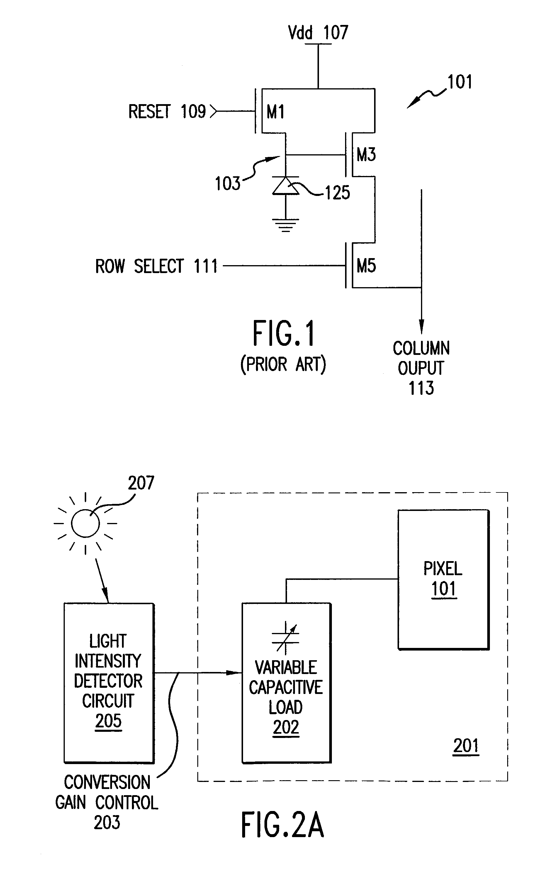
[0021]FIG. 2A shows a block diagram of a variable conversion gain pixel 201, in a preferred embodiment of the present invention. A pixel, such as the prior art pixel 101, is connected to a variable capacitive load 202. A light intensity detector circuit 205 (located outside the variable conversion gain pixel 201) senses the brightness of incident light 207, and outputs a conversion gain control signal 203 in response. The conversion gain control signal 203 adjusts the capacitance of the variable capacitive load 202 to compensate for the intensity of the incident light 207.

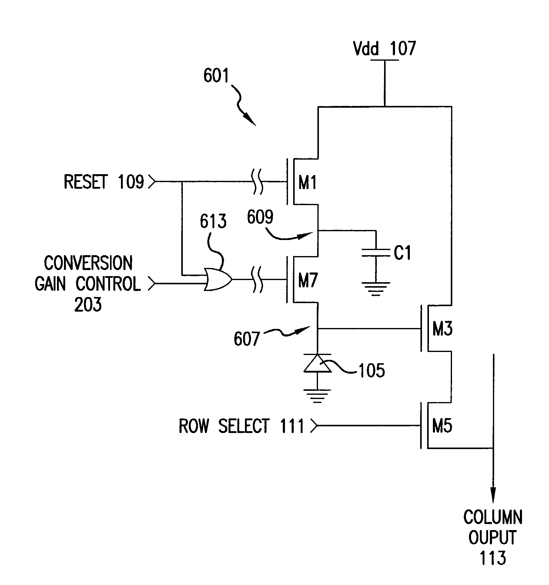
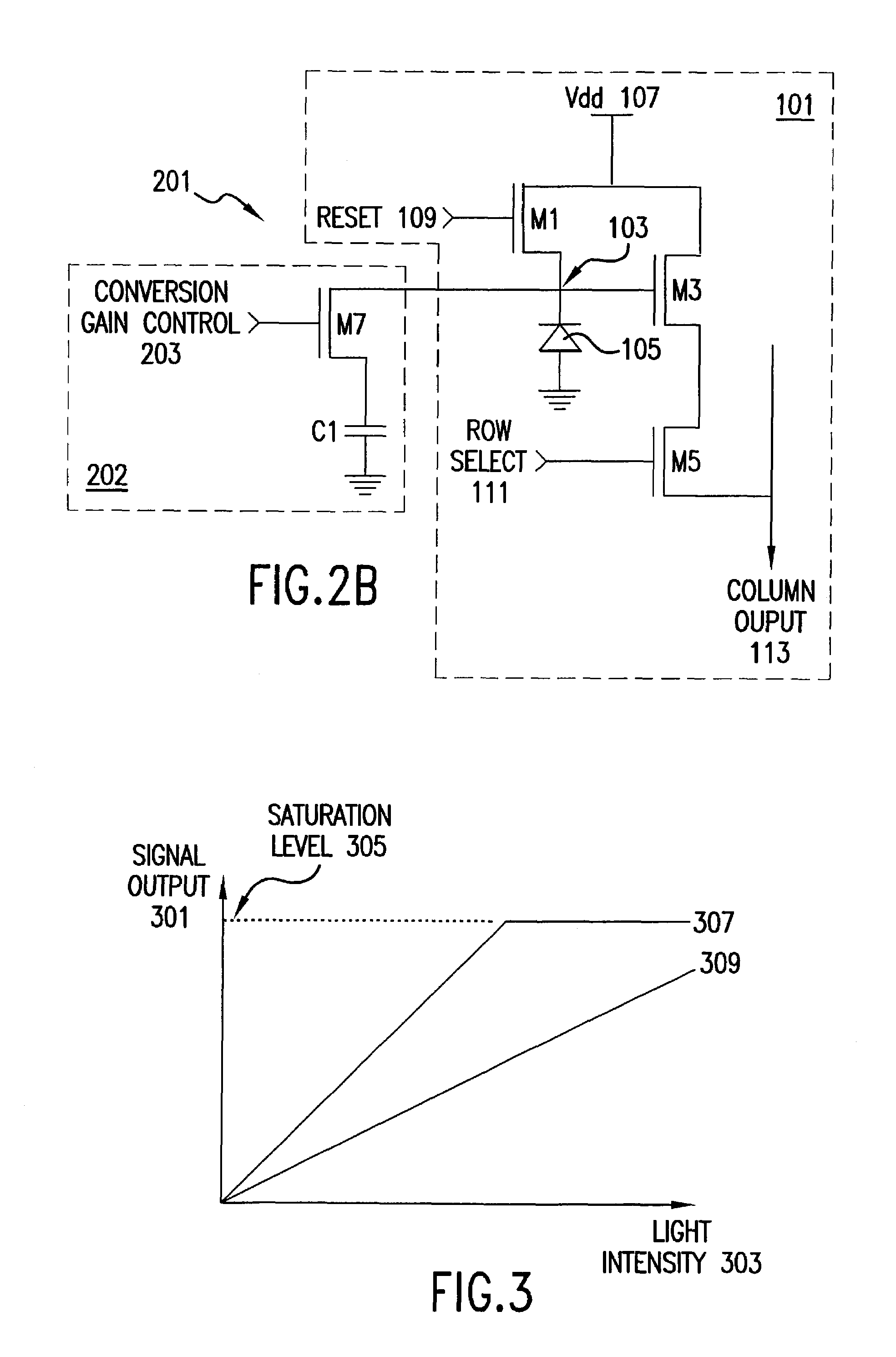
[0022]FIG. 2B shows the variable conversion gain pixel 201 of FIG. 2A in more detail. The pixel 101 is the same pixel shown in FIG. 1. The variable capacitive load 202 consists of a transistor M7 and a capacitor C1, and is connected in parallel with the photodiode 105. The transistor M7 connects the capacitor C1 to node 103 of the pixel 101. The gate of the transistor M7 is connected to the conversion gain control ...


PUM


Abstract

An image sensor pixel has variable conversion gain to prevent overexposure of the pixel without reducing the exposure period. Under dim lighting conditions, the pixel operates with high conversion gain and is highly sensitive to light. When the incident light is bright, the pixel switches into a low conversion gain, low-sensitivity mode. The variable conversion gain is implemented by connecting a variable capacitive load in parallel with the photodiode of the image sensor pixel. When the incident light intensity exceeds a certain threshold, the variable capacitive load is increased to allow the photodiode to absorb more light. Likewise, the variable capacitive load is decreased when the incident light intensity is below a certain threshold.

Description

FIELD OF THE INVENTION[0001]The invention is directed towards the field of CMOS image sensors, and more specifically, towards preventing overexposure in CMOS image sensors.BACKGROUND OF THE INVENTION[0002]CMOS image sensors are gaining widespread use as digital cameras and digital video cameras become more common. Similar to traditional film, the CMOS image sensor captures an image when exposed to light. The CMOS image sensor typically consists of a large array of pixels that are organized into rows. Normally, the pixels in the array are not all exposed to light at the same time. Rather, the pixels are exposed sequentially, row by row. This method is known as a “rolling shutter”. The exposure time for a single row of pixels is called the exposure period. The total time required to expose and process the pixels in the entire array is known as the frame period.[0003]One problem associated with the rolling shutter method is that the illumination level of the light source may vary over ...

Claims


Application Information

Patent Timeline
IPC IPC(8): H04N5/335H01L31/062H04N5/351H04N5/359H04N5/3745
CPCH04N3/155H04N25/59
Inventor YING, BOND Y.BAER, RICHARD L
Owner APTINA IMAGING CORP
Why Eureka
Try Eureka