Electrically erasable and programmable, non-volatile semiconductor memory device having a single layer of gate material, and corresponding memory plane

a semiconductor memory, non-volatile technology, applied in the direction of digital storage, instruments, transistors, etc., can solve the problems of gate oxide of the transistor, the threshold voltage of the transistor to be degraded, and the aging of the transistor

Inactive Publication Date: 2008-02-19
STMICROELECTRONICS SRL
View PDF11 Cites 24 Cited by
  • Summary
  • Abstract
  • Description
  • Claims
  • Application Information

AI Technical Summary

Benefits of technology

[0005]It is an object of the present invention to provide a memory cell structure that avoids the phenomenon of transistor aging during repeated erase cycles.
[0010]According to the invention, the structure of the memory cell is consequently completely different from the conventional structures in the sense that it has no control gate separate from the floating-gate transistor. This is because, according to the invention, it is a part of the floating-gate transistor, and more particularly the source, drain and channel regions of this transistor, that form the control gate. Moreover, during erasure of the cell, the charges are extracted no longer through the gate oxide of the floating-gate transistor but through a gate oxide (dielectric) which is located opposite an active zone electrically isolated from the active zone incorporating the control gate, and consequently the source, channel and drain regions of the floating-gate transistor. As a consequence, according to the invention, degradation of the oxide in the tunnel zone does not cause the transistor of the cell to undergo ageing.
[0018]This being the case, to facilitate erasure it may prove advantageous to provide, on the surface of the first active zone, in addition to the aforementioned contact, a surface zone having the second type of conductivity, for example P+-type conductivity, and extending around the tunnel zone. Of course, this surface zone is electrically connected to the contact zone, for example, by siliciding. Thus, a transistor, for example a PMOS transistor, whose source and drain regions are short-circuited will be produced with the first part of the gate material. This will allow that part of the active zone located beneath the first part of the gate material to be very conducting.
[0021]In the programming state, the bias means may cause hot-carrier programming within the transistor. They may also cause Fowler-Nordheim programming, by applying preferably equal voltages to the source, drain and substrate regions of the transistor that are much higher than those applied to the first active zone. Moreover, in the read state, it will be advantageous to choose a drain / source voltage difference limited to 1 volt in absolute value. This prevents very slow reprogramming of the memory cell, or else unintentional, parasitic programming of a virgin memory cell.

Problems solved by technology

However, this erase process, when it is repeated in a cyclic fashion, as is generally the case for memory applications, causes the gate oxide of the transistor and the threshold voltage of this transistor to be degraded.
In other words, repeatedly extracting the electrons through the gate oxide of the transistor eventually causes aging of the transistor.

Method used


Image

  • Electrically erasable and programmable, non-volatile semiconductor memory device having a single layer of gate material, and corresponding memory plane
  • Electrically erasable and programmable, non-volatile semiconductor memory device having a single layer of gate material, and corresponding memory plane
  • Electrically erasable and programmable, non-volatile semiconductor memory device having a single layer of gate material, and corresponding memory plane

Examples


Embodiment Construction

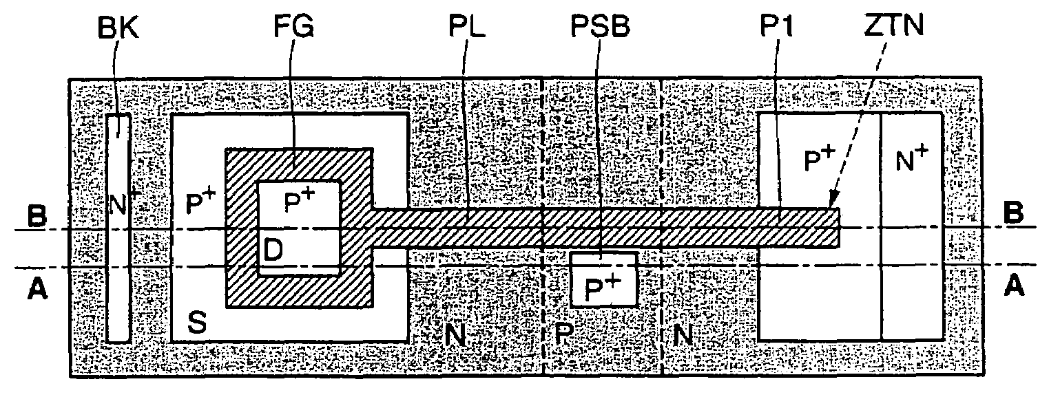
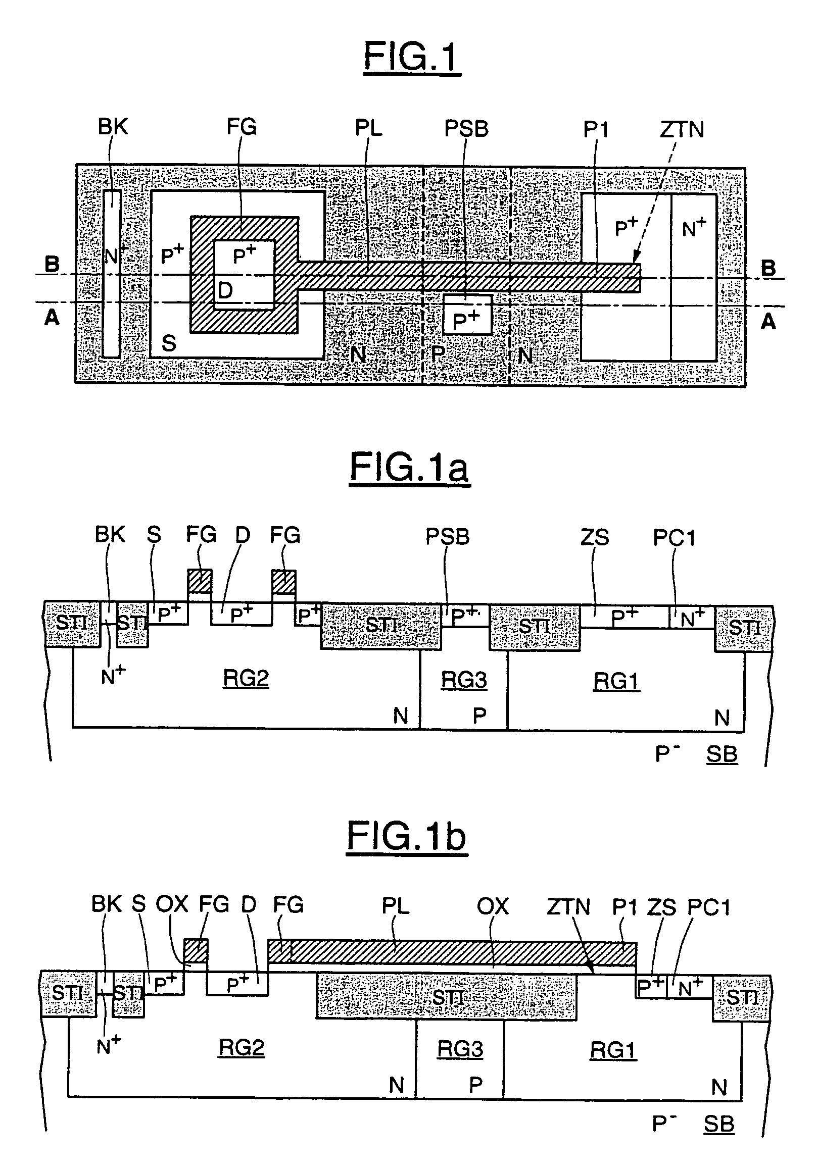
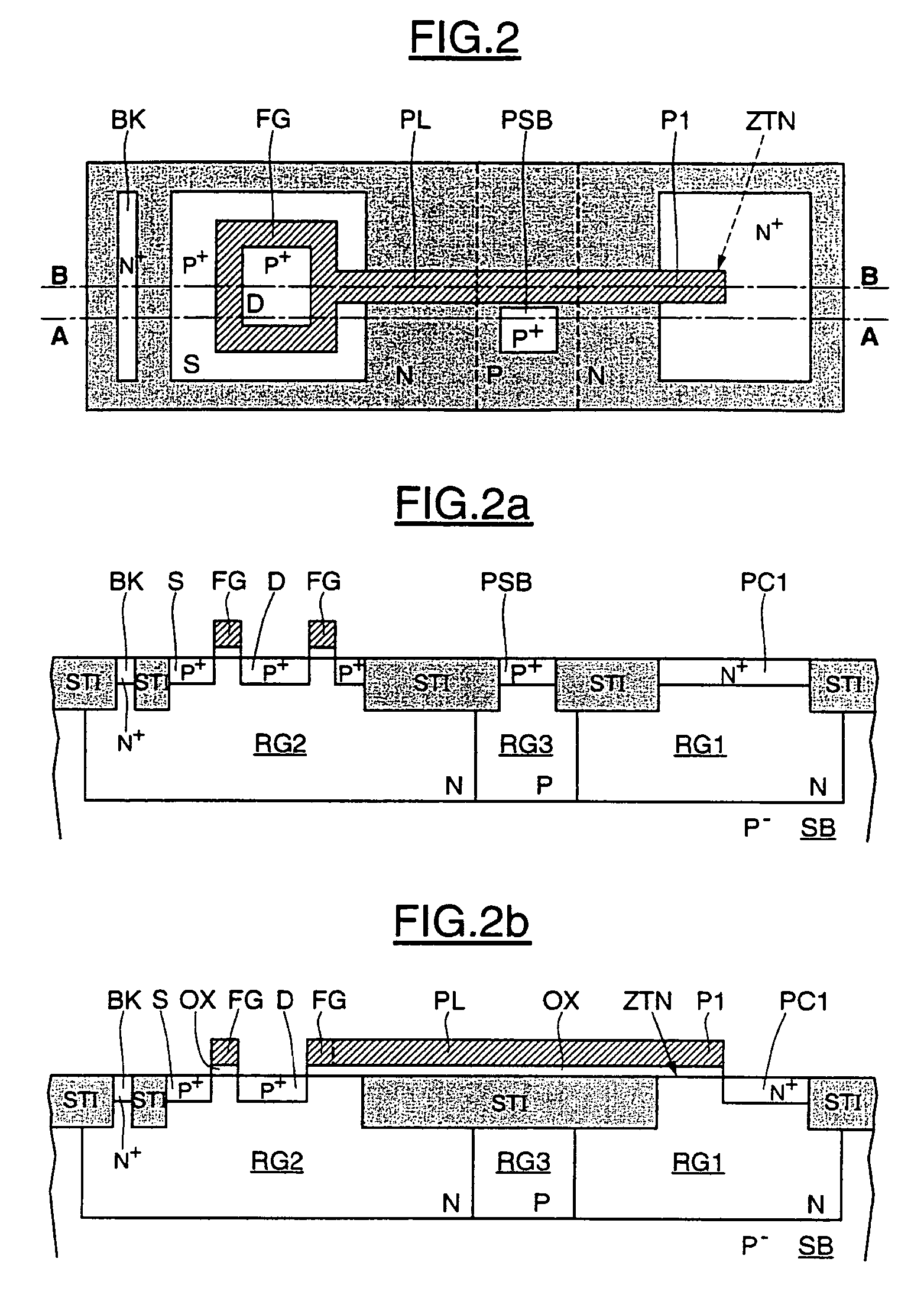
[0035]In the following, FIG. 1a (or alternatively 2a and 3a) and FIG. 1b (or alternatively 2b and 3b) are sections on the lines A-A and B-B, respectively, of FIG. 1 (or alternatively of FIG. 2 and FIG. 3). In FIGS. 1a and 1b, the reference SB denotes a semiconductor substrate, for example made of P−-doped silicon, of an integrated circuit. This substrate SB comprises a first substrate region RG1, formed from an N-doped semiconductor well, and a second substrate region RG2, formed from another N-doped semiconductor well. The two wells RG1 and RG2 are separated by a third semiconductor region RG3 formed from a P-doped well.

[0036]The well RG3 provides the mutual electrical isolation, depthwise, of the two wells RG1 and RG2. This electrical isolation is in fact produced by PN junctions that will be reverse-biased. On the surface, the mutual electrical isolation of the two wells RG1 and RG2 is provided by an isolation region STI (shallow trench isolation). The isolation region STI includ...


PUM


Abstract

The semiconductor memory device includes an electrically erasable programmable non-volatile memory cell having a single layer of gate material and including a floating-gate transistor and a control gate. The source, drain and channel regions of the floating-gate transistor form the control gate. Moreover, the memory cell includes a dielectric zone lying between a first part of the layer of gate material and a first semiconductor active zone electrically isolated from a second active zone incorporating the control gate. This dielectric zone then forms a tunnel zone for transferring, during erasure of the cell, the charges stored in the floating gate to the first active zone.

Description

FIELD OF THE INVENTION[0001]The present invention relates to integrated circuits and more particularly to semiconductor memory devices of the electrically erasable and programmable, non-volatile type having a single layer of gate material.BACKGROUND OF THE INVENTION[0002]The structure of a conventional memory cell is disclosed, for example, in U.S. Pat. No. 5,761,121 directed to a memory cell for a PMOS structure. More specifically, such a cell includes a floating-gate transistor and a control gate which is produced by implantation within a semiconductor substrate. This buried layer, which acts as control gate is capacitively coupled to the floating gate. The control gate and the floating-gate transistor are electrically isolated by an isolation zone, for example of the STI (Shallow Trench Isolation) type. The layer of gate material, generally made of polysilicon, within which the floating gate of the transistor is produced, is isolated from the active zone by a dielectric, for exam...

Claims


Application Information

Patent Timeline
Patent Type & Authority Patents(United States)
IPC IPC(8): G11C16/04H01L21/336H01L21/8247H01L27/115H01L29/788H01L29/792
CPCH01L27/115H01L27/11521H01L27/11558H01L29/66825H01L29/7881H10B41/60H10B69/00H10B41/30
Inventor GENDRIER, PHILIPPEDRAY, CYRILLEFOURNEL, RICHARDPOIRIER, SEBASTIENCASPAR, DANIELCANDELIER, PHILIPPE
Owner STMICROELECTRONICS SRL
Why Eureka
Try Eureka