
Eureka
For R&D, Eureka makes reading and utilizing patents & technical documents easy.
Eureka AIR
Designed for self-driven R&D workflows. Generate viable solutions, solve complex R&D challenges, empower your innovation with AI.

Eureka Materials
Designed for material experts only. Revolutionize your material R&D, from search, analyze, to developing new materials.

TechResearch
Generate reliable direction feasibility study reports for your R&D in just a few steps.

TechSeek
Discover and master advanced knowledge NOW. Basics, ideas, possibilities, all at once.

TechMind
As an expert in R&D Theories, TechMind can generates customized viable solutions instantly.

TechRisk
Analyze your overall solution with one click, know your potential R&D risks in advance.

TechMonitor
Get weekly tech updates, stay abreast of the latest tech innovations and key insights.
Optical disk playback apparatus and data playback method therefor
- Summary
- Abstract
- Description
- Claims
- Application Information
AI Technical Summary
Benefits of technology
Problems solved by technology
Method used
Image

Examples
first embodiment
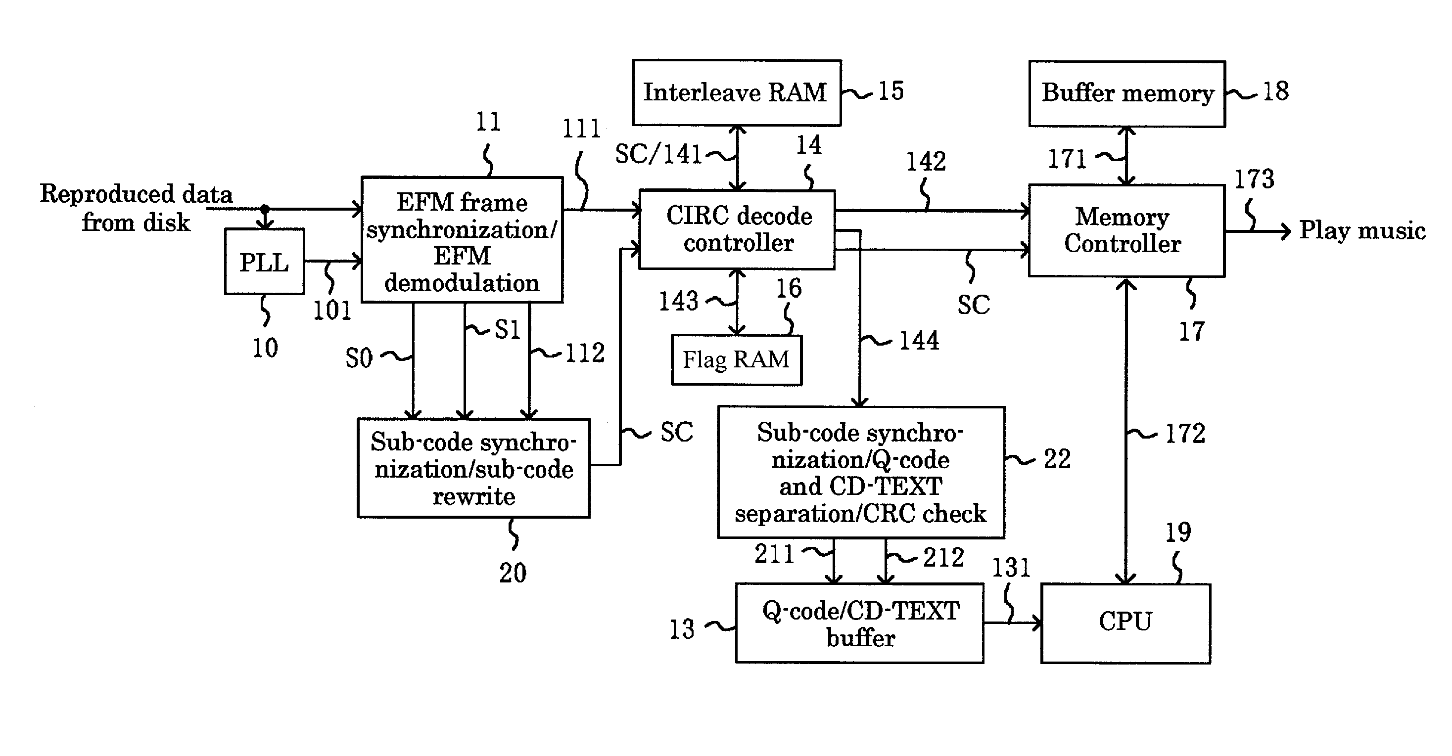
[0070]FIG. 4 illustrates the configuration of an optical disk playback apparatus according to the present invention, and FIG. 5 illustrates the configuration of a memory address management circuit in a CIRC decode controller provided in the optical disk playback apparatus.
[0071]In optical disk playback apparatus 1, data read from a disk such as a CD (compact disk) is applied to EFM (Eight-to-Fourteen Modulation) frame synchronization / EFM demodulation circuit 11 and to PLL (Phase Locked Loop) circuit 10. EFM frame synchronization / EFM demodulation circuit 11 is also applied with bit clock 101 generated by PLL circuit 10.
[0072]EFM frame synchronization / EFM demodulation circuit 11 delivers 8-bit main data 111 decoded from main data 111, which has a length of 16 bits upon modulation, to CIRC decode controller 14. EFM frame synchronization / EFM demodulation circuit 11 also delivers signals indicative of synchronization information S0, S1 of sub-codes as well as sub-code symbol bits (P to Q...
second embodiment
[0142]Next, description will be made on an optical disk playback apparatus according to the present invention.
[0143]In the apparatus of the first embodiment described above, additionally stored in interleave RAM 15 is only minimum 1-bit sub-code synchronization signal SC after synchronization information S0, S1 is protected for synchronization. However, since interleave RAM 15 has a data width of eight bits, it can store up to seven bits of other data. Therefore, a Q-code CRC determination result may be stored in one of the seven bits together with sub-code synchronization signal SC. The optical disk playback apparatus of the second embodiment differs from the apparatus of the first embodiment in that data other than 1-bit sub-code synchronization signal SC are additionally stored in the interleave RAM.
[0144]Referring to FIG. 8 which shows other exemplary assignments of addresses in a symbol area within the interleave RAM in the second embodiment, only sub-code synchronization signa...
third embodiment
[0155]Next, description will be made on an optical disk apparatus according to the present invention.
[0156]In the aforementioned apparatus of the first embodiment, the address management for sub-code synchronization signal SC stored in interleave RAM 15 uses 20 addresses, as is the case with the 28th symbol which presents the shortest interleave delay of 0×D. However, for synchronizing sub-code synchronization signal SC read from interleave RAM 15 with main data 141, the delay control having margin addresses and involving a FIFO operation is only needed to be similar to the address management for main data in the storage of sub-code synchronization signal SC in interleave RAM 15. As can be understood as well from FIGS. 11A to 11E for describing how an underflow or an overflow occurs in a FIFO area, later described, when there are (6+6) margin addresses, only two addresses are required for a data write address and a data read address, in which case a sub-code synchronization signal s...
PUM
 Abstract
Description
Claims
Application Information
 - R&D Engineer
- R&D Manager
- IP Professional
- Industry Leading Data Capabilities
- Powerful AI technology
- Patent DNA Extraction
Browse by: Latest US Patents, China's latest patents, Technical Efficacy Thesaurus, Application Domain, Technology Topic, Popular Technical Reports.
© 2024 PatSnap. All rights reserved.Legal|Privacy policy|Modern Slavery Act Transparency Statement|Sitemap|About US| Contact US: help@patsnap.com