Embedded substrate interconnect for underside contact to source and drain regions
a technology of drain region and substrate, applied in the field of semiconductor processing, can solve the problems of limiting the switching speed of transistors, limiting the arrangement of metallization structures, and occupying valuable die spa
- Summary
- Abstract
- Description
- Claims
- Application Information
AI Technical Summary
Benefits of technology
Problems solved by technology
Method used
Image


Examples
Embodiment Construction
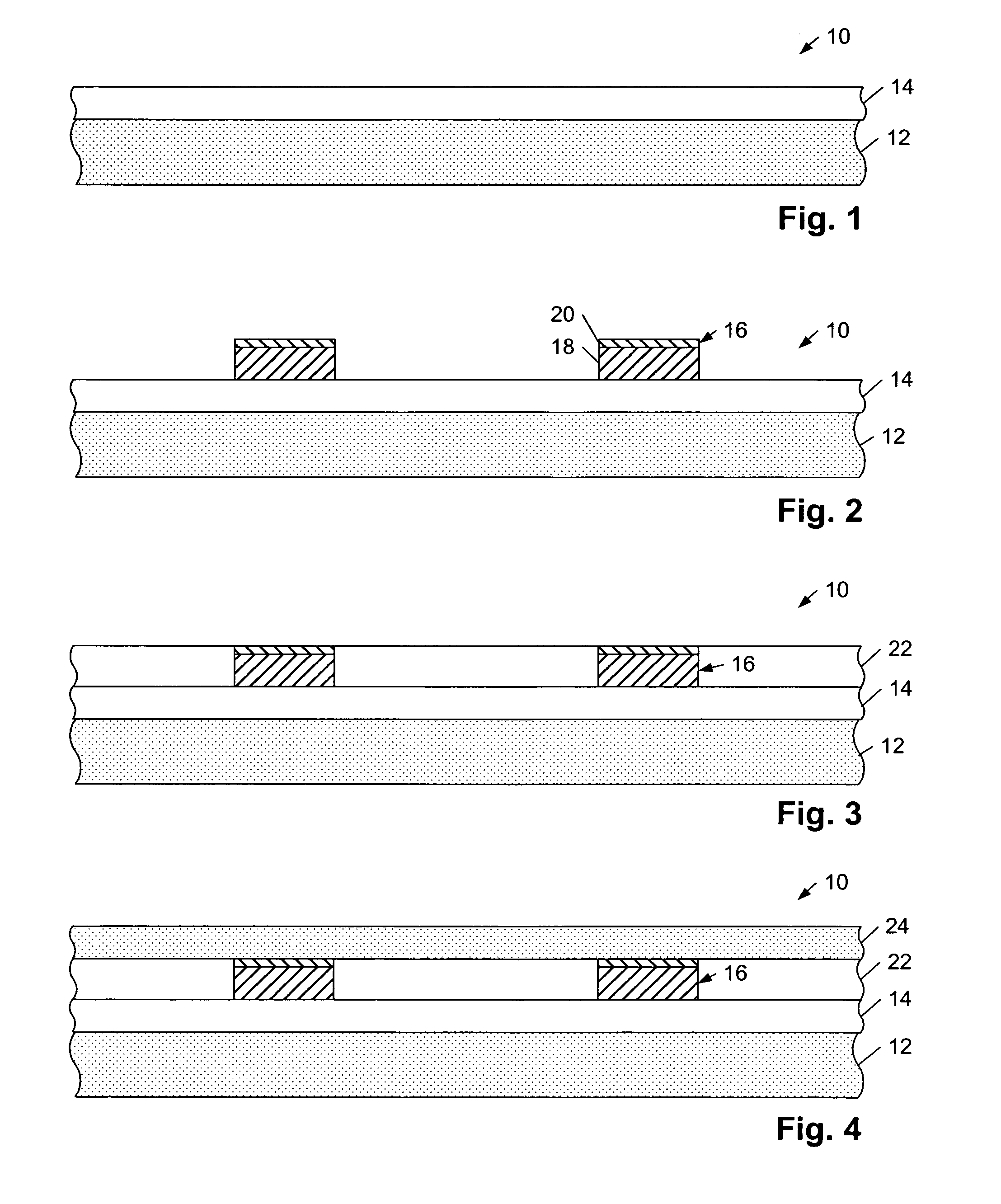
[0017]With regard to the drawings, an exemplary method for fabricating a semiconductor-on-insulator (SOI) substrate with an embedded conductive line is shown in FIGS. 1-4. In addition, FIGS. 5-7 illustrate a method for processing a SOI substrate having an embedded conductive line such that one of a pair of source and drain regions extends through an upper semiconductor layer of the SOI substrate to the conductive line. As used herein, an “upper” semiconductor layer of a SOI substrate refers to the layer within the substrate above which devices, such as transistors, are most remotely formed or slated to be formed. Therefore, the orientation of a semiconductor topography including such a substrate (i.e., whether the topography is arranged sideways, flipped, or upright relative to the position of the upper semiconductor layer within the substrate) does not affect the reference of the upper semiconductor layer. In other words, the upper semiconductor layer of a SOI substrate may not nec...
PUM
 Abstract
Description
Claims
Application Information
 - R&D
- Intellectual Property
- Life Sciences
- Materials
- Tech Scout
- Unparalleled Data Quality
- Higher Quality Content
- 60% Fewer Hallucinations
Browse by: Latest US Patents, China's latest patents, Technical Efficacy Thesaurus, Application Domain, Technology Topic, Popular Technical Reports.
© 2025 PatSnap. All rights reserved.Legal|Privacy policy|Modern Slavery Act Transparency Statement|Sitemap|About US| Contact US: help@patsnap.com