Mirror device with anti-reflective coating layer and method for manufacturing the same

a mirror device and anti-reflective technology, applied in the field of mirror devices with anti-reflective coating layers and methods for manufacturing the same, can solve the problems of poor relative contrast, inability to solve problems caused by fringe effects, poor black pixel state, etc., to reduce the influence of electromagnet interference, reduce the bad influence of fringe effects, and reduce the effect of poor fringe effects

Active Publication Date: 2008-03-18
HIMAX TECH LTD
View PDF3 Cites 0 Cited by
  • Summary
  • Abstract
  • Description
  • Claims
  • Application Information

AI Technical Summary

Benefits of technology

[0011]The mirror device of the invention has the anti-reflective coating layer on the mirror layer, which can shield the bright band area caused by fringe effect, so as to minimize the bad influence of the fringe effect. The circuit layer at the same height as the mirror layer, due to the anti-reflective coating layer covered on the circuit layer, can decrease the influence of electromagnet interference. In manufacture, the method of the invention follows the semiconductor manufacturing process, and has high precision and simple process.

Problems solved by technology

Since the conventional liquid crystal display (LCD) has a fringe effect on the black and white boundary area, a bright band will be caused in the area that originally should be fully black, resulting in a poor black pixel state, and thereby a poor relative contrast.
In the liquid crystal on silicon (LCoS), since the size of pixel is too small (approximately 10 μm) to add a suitable black matrix to shield the bright band area, the problems caused by the fringe effect can't be solved.

Method used


Image

  • Mirror device with anti-reflective coating layer and method for manufacturing the same
  • Mirror device with anti-reflective coating layer and method for manufacturing the same
  • Mirror device with anti-reflective coating layer and method for manufacturing the same

Examples


first embodiment

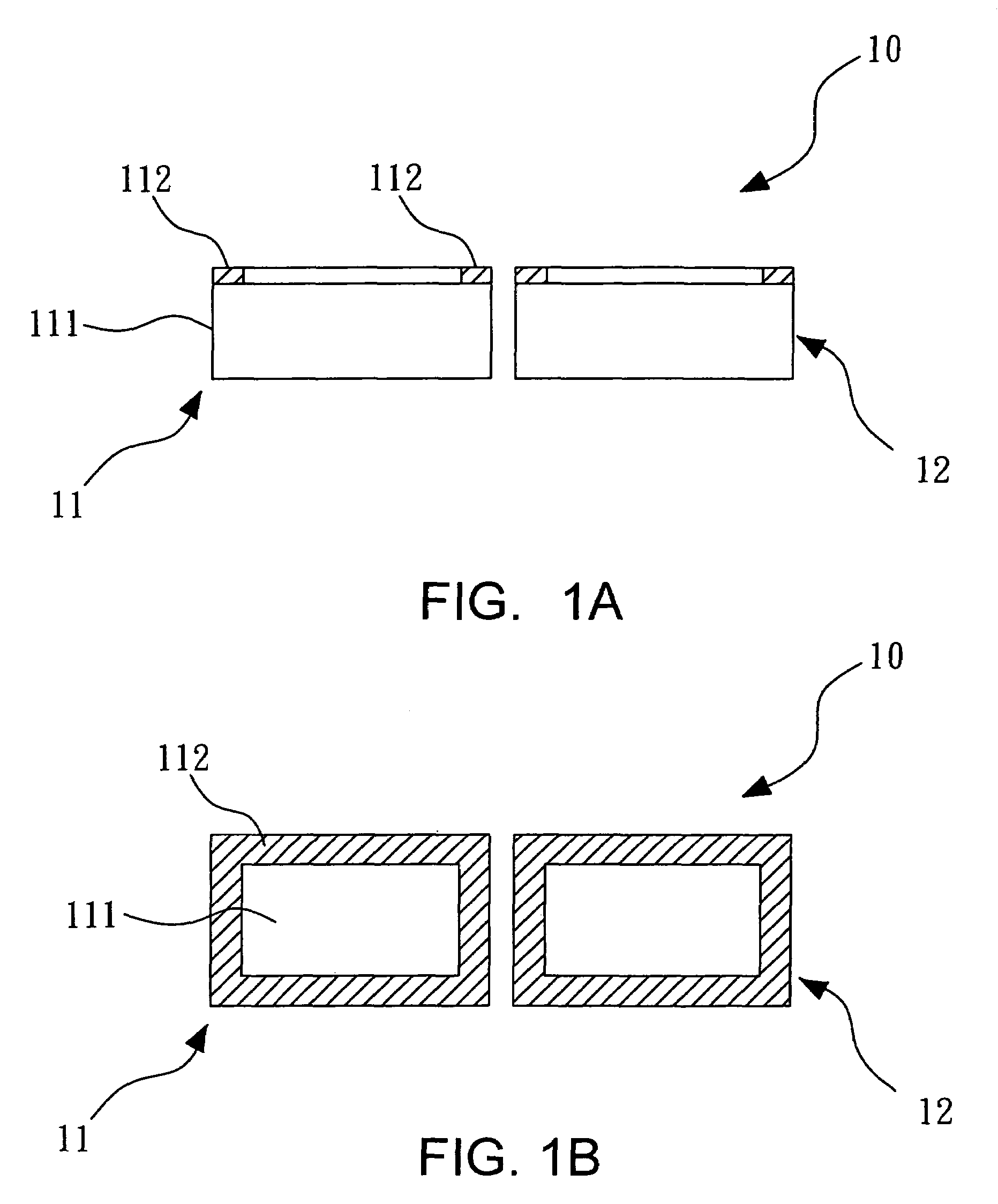
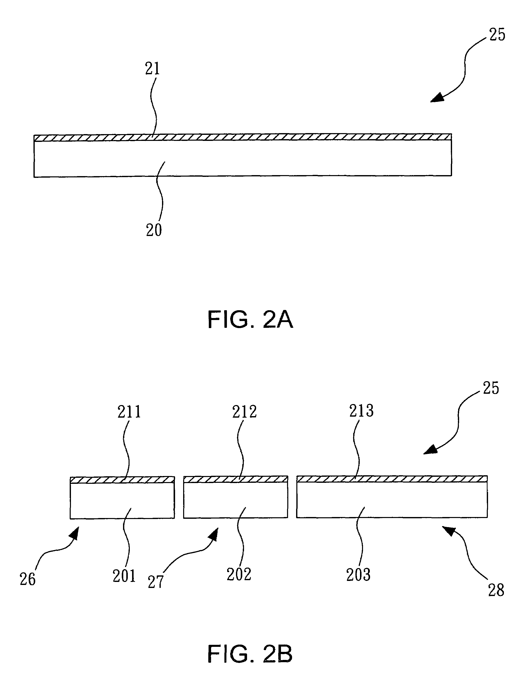
[0020]Referring to the FIGS. 2A-2D, schematic views of manufacture method of the mirror device with anti-reflective coating layer according to the invention are shown. First referring to FIG. 2A, an anti-reflective metal film 21 is formed on a first surface of a mirror material 20 to be a mirror device 25. The mirror material 20 can be a metal material, and the anti-reflective metal film 21 can be an anti-reflective material, e.g., titanium nitride (TiN) etc. Referring to the FIG. 2B, a plurality of mirror units 26 and 27 are defined from the mirror device 25. Each mirror unit has a mirror layer and an anti-reflective metal film unit, the anti-reflective metal film unit is formed on a first surface of the mirror layer. Taking the mirror unit 26 as an example, the mirror unit 26 has a mirror layer 201 and an anti-reflective metal film unit 211. The anti-reflective metal film unit 211 is formed on a first surface of the mirror layer 201. The mirror units 26 and 27 are preferably forme...

third embodiment

[0027]Referring to FIGS. 4A-4E, schematic views of manufacture method of the mirror device with anti-reflective coating layer according to the invention. First referring to FIG. 4A, a plurality of mirror layers 401 and 402 is defined from a mirror material. There is a gap between the mirror layers 401 and 402. Preferably, the mirror material is cut to form the mirror layers 401 and 402. Referring to FIG. 4B, a light absorption material 411 is filled into the gap between the mirror layers 401 and 402. Referring to FIG. 4C, an isolation layer 42 is formed on a first surface of the mirror layers 401 and 402, and an anti-reflective metal film 43 is formed on a first surface of the isolation layer 42.

[0028]Referring to FIG. 4D, an isolation coating layer 421 and an anti-reflective coating layer 431 is defined from the isolation layer 42 and the anti-reflective metal film 43. The isolation coating layer 421 and the anti-reflective coating layer 431 are formed on edges of the first surface...


PUM

PropertyMeasurementUnit
sizeaaaaaaaaaa
heightaaaaaaaaaa

Abstract

The invention relates to a method for manufacturing a mirror device with anti-reflective coating layer. The method of the invention comprises: (a) forming an anti-reflective metal film on a first surface of a mirror material to be a mirror device; (b) defining a plurality of mirror units from the mirror device, each mirror unit having a mirror layer and an anti-reflective metal film unit, the anti-reflective metal film unit formed on a first surface of the mirror layer; and (c) defining an anti-reflective coating layer from the anti-reflective metal film unit, the anti-reflective coating layer formed on edges of the first surface of the mirror layer. According to the invention, the anti-reflective coating layer on the mirror layer can shield a bright area caused by fringe effect so as to minimize the bad influence of the fringe effect. In manufacture, the method of the invention follows the semiconductor manufacturing process, and has high precision and simple process.

Description

BACKGROUND OF THE INVENTION[0001]1. Field of the Invention[0002]The present invention relates to a display, and particularly to a mirror device with anti-reflective coating layer and method for manufacturing the same.[0003]2. Description of the Related Art[0004]Since the conventional liquid crystal display (LCD) has a fringe effect on the black and white boundary area, a bright band will be caused in the area that originally should be fully black, resulting in a poor black pixel state, and thereby a poor relative contrast. In the conventional TFT LCD technology, the bright band area can be shielded by adding a black matrix, so as to improve the disadvantages caused by the fringe effect.[0005]Referring to FIG. 5, a structural schematic view of the conventional liquid crystal on silicon (LCoS) is shown. The conventional liquid crystal on silicon 50 mainly comprises: a substrate 51, a storage capacitor 52, a pixel switch 53, a first metal layer (Metal 1) 54, a second metal layer (Metal...

Claims


Application Information

Patent Timeline
Patent Type & Authority Patents(United States)
IPC IPC(8): G02B26/00
CPCG02B1/11G02B5/0816
Inventor CHEN, WEI-HSIAO
Owner HIMAX TECH LTD
Why Eureka
Try Eureka