Mirror device with anti-reflective coating layer and method for manufacturing the same
a mirror device and anti-reflective technology, applied in the field of mirror devices with anti-reflective coating layers and methods for manufacturing the same, can solve the problems of poor relative contrast, inability to solve problems caused by fringe effects, poor black pixel state, etc., to reduce the influence of electromagnet interference, reduce the bad influence of fringe effects, and reduce the effect of poor fringe effects
- Summary
- Abstract
- Description
- Claims
- Application Information
AI Technical Summary
Benefits of technology
Problems solved by technology
Method used
Image
Examples
first embodiment
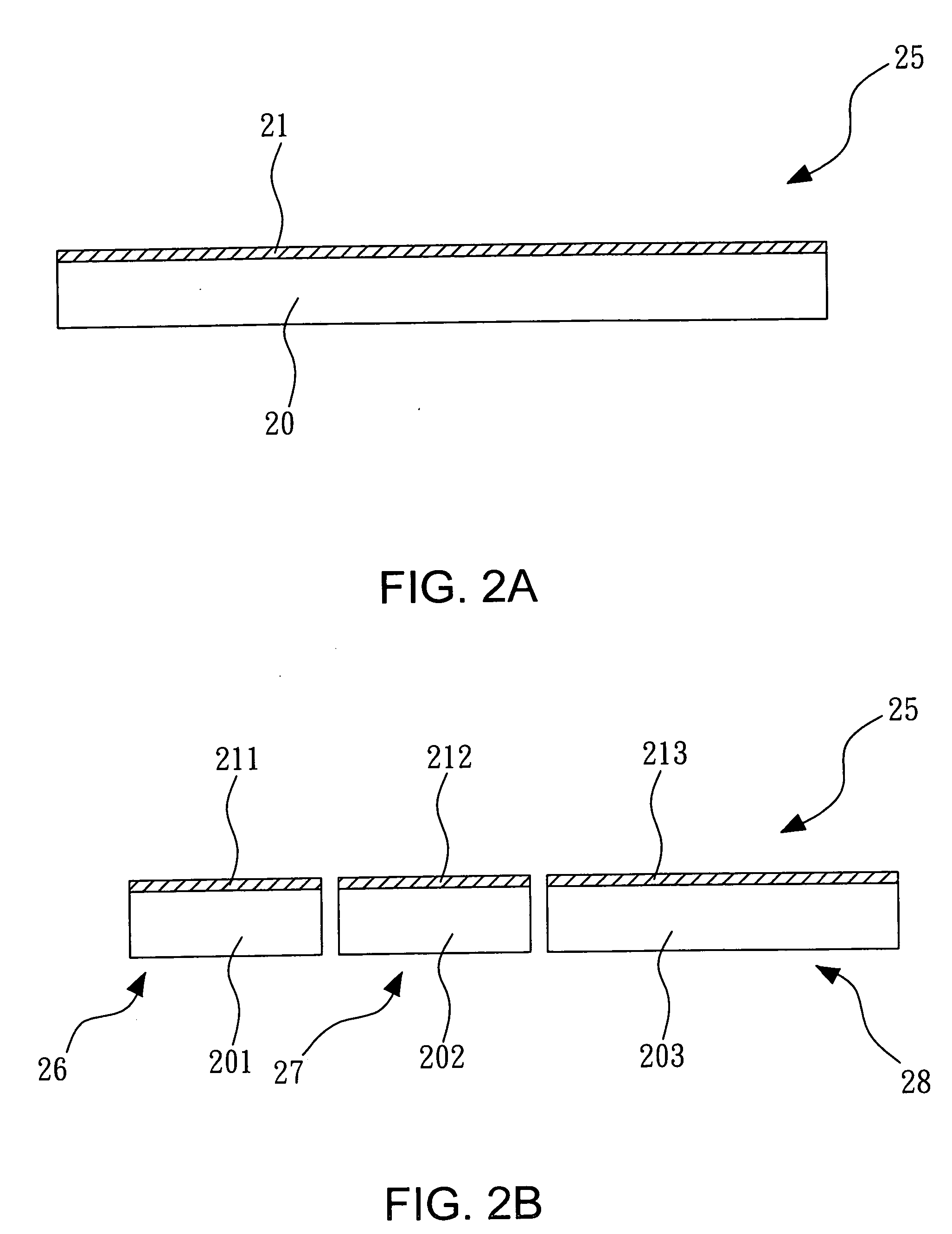
[0020] Referring to the FIGS. 2A-2D, schematic views of manufacture method of the mirror device with anti-reflective coating layer according to the invention are shown. First referring to FIG. 2A, an anti-reflective metal film 21 is formed on a first surface of a mirror material 20 to be a mirror device 25. The mirror material 20 can be a metal material, and the anti-reflective metal film 21 can be an anti-reflective material, e.g., titanium nitride (TiN) etc. Referring to the FIG. 2B, a plurality of mirror units 26 and 27 are defined from the mirror device 25. Each mirror unit has a mirror layer and an anti-reflective metal film unit, the anti-reflective metal film unit is formed on a first surface of the mirror layer. Taking the mirror unit 26 as an example, the mirror unit 26 has a mirror layer 201 and an anti-reflective metal film unit 211. The anti-reflective metal film unit 211 is formed on a first surface of the mirror layer 201. The mirror units 26 and 27 are preferably form...
third embodiment
[0027] Referring to FIGS. 4A-4E, schematic views of manufacture method of the mirror device with anti-reflective coating layer according to the invention. First referring to FIG. 4A, a plurality of mirror layers 401 and 402 is defined from a mirror material. There is a gap between the mirror layers 401 and 402. Preferably, the mirror material is cut to form the mirror layers 401 and 402. Referring to FIG. 4B, a light absorption material 411 is filled into the gap between the mirror layers 401 and 402. Referring to FIG. 4C, an isolation layer 42 is formed on a first surface of the mirror layers 401 and 402, and an anti-reflective metal film 43 is formed on a first surface of the isolation layer 42.
[0028] Referring to FIG. 4D, an isolation coating layer 421 and an anti-reflective coating layer 431 is defined from the isolation layer 42 and the anti-reflective metal film 43. The isolation coating layer 421 and the anti-reflective coating layer 431 are formed on edges of the first surfa...
PUM
| Property | Measurement | Unit |
|---|---|---|
| size | aaaaa | aaaaa |
| height | aaaaa | aaaaa |
Abstract
Description
Claims
Application Information


