Solid-state imaging device and driving method as well as electronic appartus

a technology of solid-state imaging and driving method, which is applied in the direction of instruments, television systems, and scanning details of television systems, can solve problems such as bad influence on signal reading, and achieve the effects of reducing noise generation, reducing noise, and high simultaneity in degree of freedom

Active Publication Date: 2013-04-02
SONY SEMICON SOLUTIONS CORP
View PDF13 Cites 9 Cited by
  • Summary
  • Abstract
  • Description
  • Claims
  • Application Information

AI Technical Summary

Benefits of technology

[0011]However, in a video signal in recent years, increase of the number of pixels and the frame rate has been and is advancing, and the row period tends to become short. For example, in high definition television standards for imaging and displaying a dynamic picture formed from an image of 1,920 pixels horizontally and 1,080 pixels vertically at a frame rate of 1 / 60 second, the row period is 7.6 microseconds. Thus, the rate at which the overflow gate driving occupies in the transition is high, and the period which can be secured is very short.
[0013]Therefore, it is desirable to provide a solid-state imaging device and a driving method for a solid-state imaging device as well as an electronic apparatus wherein simultaneous driving of overflow gates is carried out upon sequential reading out operation such that, while an accumulation period having high simultaneity in degree of freedom in time is provided, a bad influence of the simultaneous driving is minimized thereby to reduce noise included in a picked up image.
[0031]With the solid-state imaging device and the driving method for a solid-state imaging device as well as the electronic apparatus, simultaneous driving of overflow gates can be carried out upon sequential reading out operation such that, while an accumulation period having high simultaneity in degree of freedom in time is provided, a bad influence of the simultaneous driving is minimized thereby to reduce noise included in a picked up image.
[0032]In summary, with the solid-state imaging device and the driving method for a solid-state imaging device as well as the electronic apparatus, when an image is picked up using the image sensor, generation of noise can be reduced.

Problems solved by technology

Therefore, a bad influence is had on reading of a signal such that an IR drop of a power supply line occurs or a different signal line is influenced by coupling by transition of a signal over the overall area of the pixel.

Method used


Image

  • Solid-state imaging device and driving method as well as electronic appartus
  • Solid-state imaging device and driving method as well as electronic appartus
  • Solid-state imaging device and driving method as well as electronic appartus

Examples


first embodiment

Example of a Configuration of a Solid-State Imaging Device

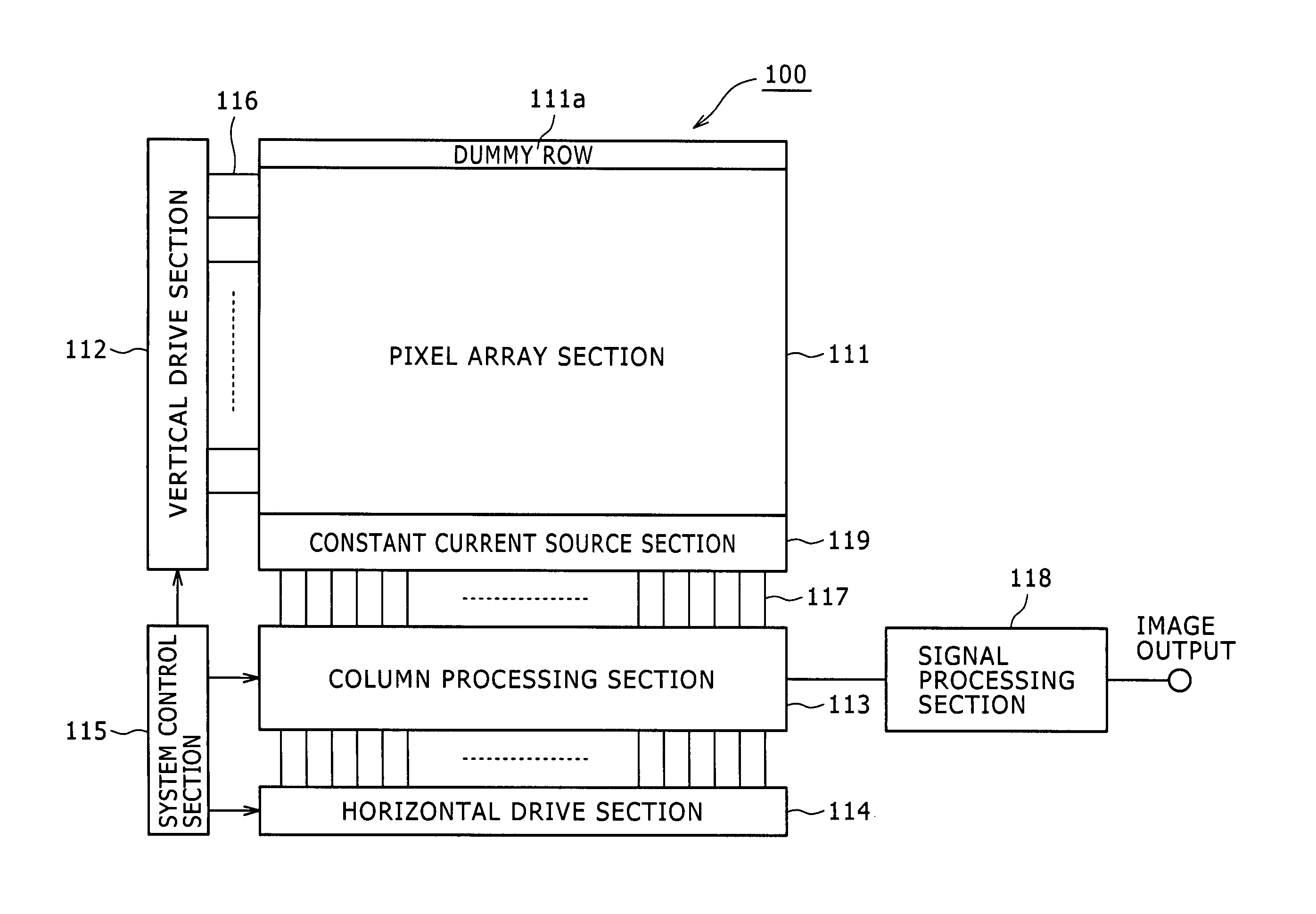
[0054]FIG. 3 is a block diagram showing an example of a configuration of a CMOS image sensor as a solid-state imaging device to which the present invention is applied.

[0055]Referring to FIG. 3, the CMOS image sensor 100 shown includes a pixel array section 111, a vertical drive section 112, a column processing section 113, a horizontal drive section 114, and a system control section 115. The pixel array section 111, vertical drive section 112, column processing section 113, horizontal drive section 114 and system control section 115 are formed on a semiconductor substrate or chip not shown. A constant current supply section 119 is provided on the pixel array section 111.

[0056]The pixel array section 111 includes a plurality of unit pixels disposed two-dimensionally in a matrix, that is, in rows and columns. Each of the unit pixels includes a photoelectric conversion element for generating photocharge of a charge amount in acc...

second embodiment

Other Examples of the Configuration of the Solid-State Imaging Device

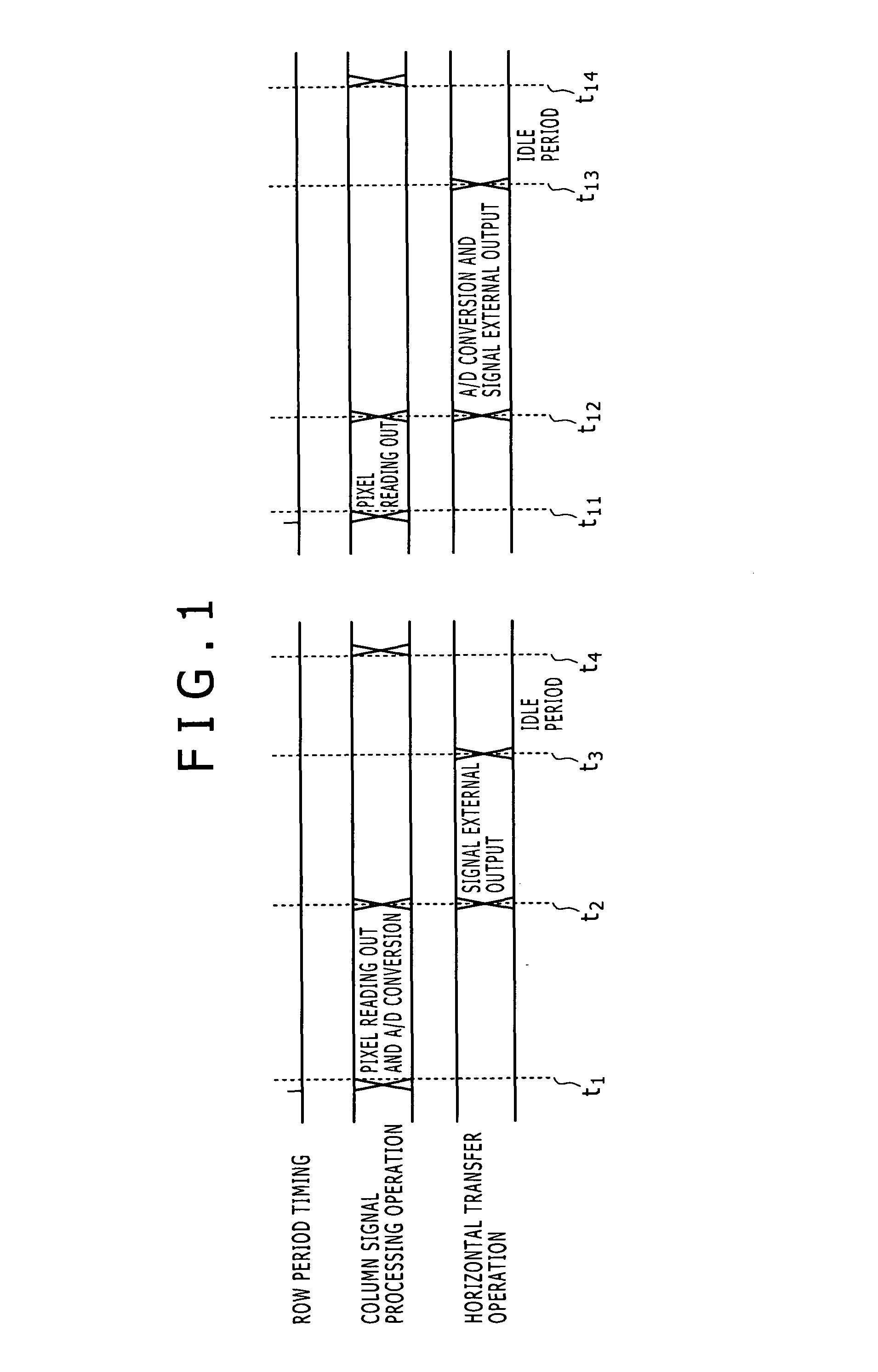
[0116]In the foregoing description, a dummy row of a configuration same as that of pixels which contribute to image display is provided and a reading out process of the dummy row is executed compulsorily at a timing at which an influence of noise is liable to be had thereby to avoid reading out at the timing at which an influence of noise is liable to be had. However, since only it is necessary to carry out reading out of a row of pixels which do not contribute to image display, for example, at a timing at which an influence of noise is liable to be had, reading out from a row whose reception light signal has been read out once may be carried out again.

[0117]FIG. 8 shows an example of a configuration of a CMOS image sensor 100 wherein a reception light signal of a row from which the reception light signal is read out once is read out again.

[0118]In particular, the CMOS image sensor 100 of FIG. 8 is similar in confi...

third embodiment

Other Examples of the Configuration of the Solid-State Imaging Device

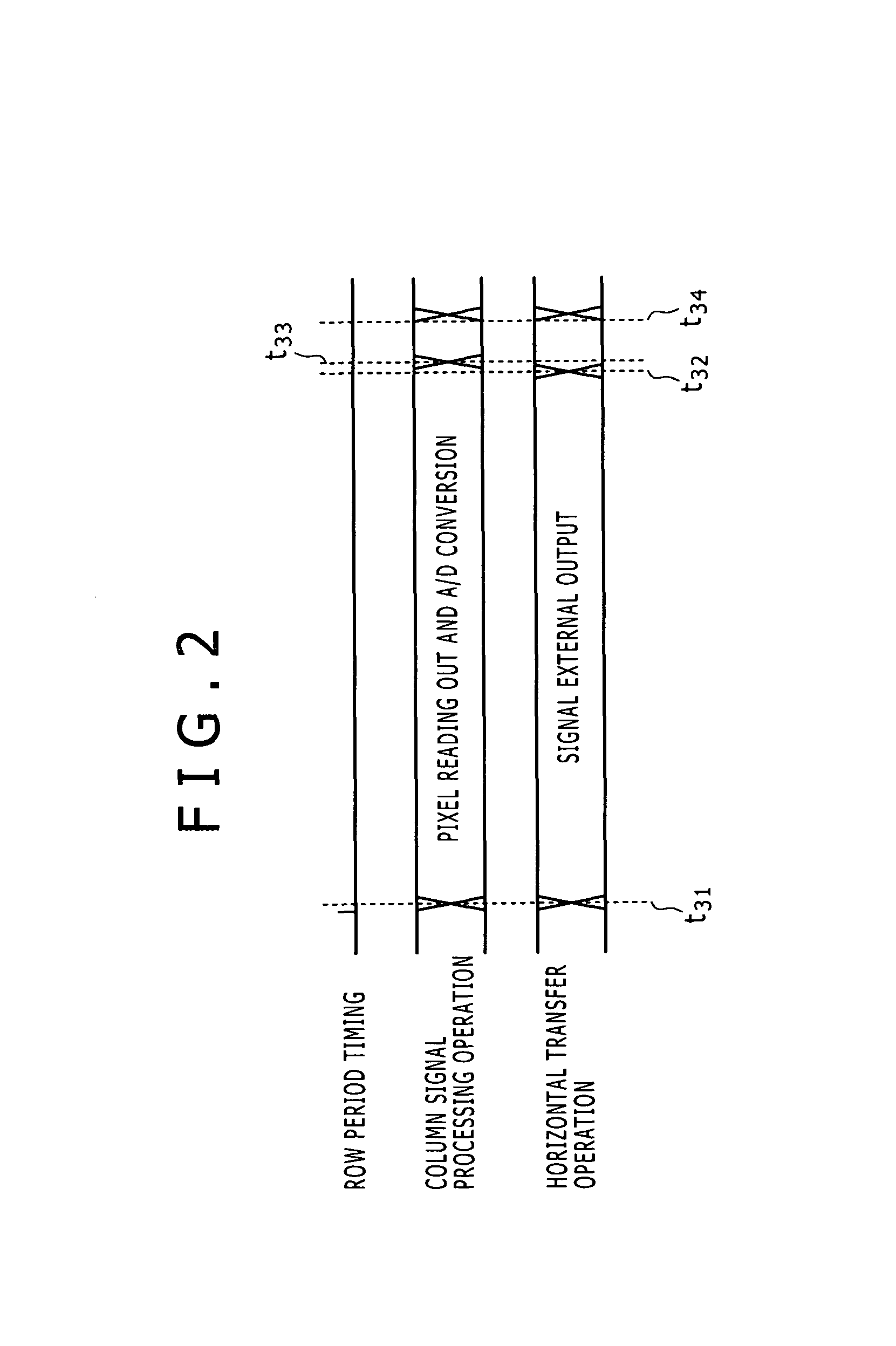
[0129]In the foregoing description, an example is described wherein a reading out process for a row same as a row formed from pixels from which a reception light signal is read out already and which do not contribute to image display at a timing at which an influence of noise is liable to be had is carried out compulsorily to avoid reading out at a timing at which an influence of noise is liable to be had. However, in the case where the countermeasure described is taken, a timing at which a reception light signal of an unnecessary row is read out is generated, and consequently, image signals are supplied discontinuously. Therefore, it is necessary in signal processing on the succeeding stage to carry out such an additional process as to remove the unnecessary row. Therefore, a line memory and a selector may be provided so that image signals are supplied continuously.

[0130]FIG. 11 shows an example of a configuration...


PUM

PropertyMeasurementUnit
chargeaaaaaaaaaa
speedaaaaaaaaaa
areaaaaaaaaaaa

Abstract

A solid-state imaging device includes: a CMOS image sensor including a plurality of pixels disposed in an array and each including a light reception element, a discharging unit, a charge accumulation section, a transfer unit, a reset unit, an amplification unit, and a selection unit; and a control unit adapted to generate a selection pulse for rendering the selection unit operative to control operation of the CMOS image sensor.

Description

BACKGROUND OF THE INVENTION[0001]1. Field of the Invention[0002]This invention relates to a solid-state imaging device and a driving method for a solid-state imaging device as well as an electronic apparatus, and more particular to a technique for reducing generation of noise in a solid-state imaging device and a driving method for a solid-state imaging device as well as an electronic apparatus.[0003]2. Description of the Related Art[0004]A popular image sensor of the CMOS (Complementary Metal Oxide Semiconductor) type includes a mechanism for sequentially scanning a pixel array, in which pixels are arrayed two-dimensionally, for each pixel row to carry out reading out. This row-sequential scanning generates a displacement in time among accumulation periods with regard to different pixel rows and gives rise to occurrence of a phenomenon called focal plane distortion that a picked up image upon imaging of a moving imaging object is distorted.[0005]In imaging applications to an imagin...

Claims


Application Information

Patent Timeline
Patent Type & Authority Patents(United States)
IPC IPC(8): H04N3/14H04N5/335H01J40/00C12Q1/68
CPCH01L27/14609H01L27/14656H04N5/357H04N5/3592H04N5/361H04N5/3532H01L27/14643H04N25/531H04N25/622H04N25/63H04N25/60
Inventor KATO, AKIHIKOOIKE, YUSUKE
Owner SONY SEMICON SOLUTIONS CORP
Why Eureka
Try Eureka