Fin-type field effect transistor

a transistor and field effect technology, applied in transistors, semiconductor devices, electrical equipment, etc., can solve the problems of increasing capacitance, destroying fet, and reducing resistance, so as to reduce capacitance, prevent high voltage destruction, and reduce fin resistance

Active Publication Date: 2008-03-25
AURIGA INNOVATIONS INC
View PDF20 Cites 73 Cited by
  • Summary
  • Abstract
  • Description
  • Claims
  • Application Information

AI Technical Summary

Benefits of technology

[0006]The present invention provides embodiments of an improved FinFET structure and the associated methods of making the embodiments of the structure. In one embodiment FinFET drive current is optimized by configuring the FinFET asymmetrically to decrease fin resistance between the gate and the source region and to decrease capacitance between the gate and the drain region. In another embodiment device destruction at high voltages is prevented by ballasting the FinFET. Specifically, resistance is increased in the fin between the gate and both the source region and the drain region so that the FinFET is operable at a predetermined maximum voltage. When multiple ballasted FinFETs of the invention are formed in a series, this ballasting prevents a premature runaway in one fin, causing destruction of the FinFET.

Problems solved by technology

However, widening the fin between the gate and the drain region not only decreases the resistance between the gate and the drain, it also increases capacitance.
In a related problem, at very high voltages a FinFET can enter a mode known as snap-back in which thermal run-away in the hottest region of a transistor channel can destroy the FET.
In a FinFET comprising a plurality of fins, if one fin enters into a breakdown condition, thermal run-away, can occur, which results in that fin conducting all additional current and ultimately resulting in the destruction of the FinFET.

Method used


Image

  • Fin-type field effect transistor
  • Fin-type field effect transistor
  • Fin-type field effect transistor

Examples


Embodiment Construction

[0033]The present invention and the various features and advantageous details thereof are explained more fully with reference to the non-limiting embodiments that are illustrated in the accompanying drawings and detailed in the following description. It should be noted that the features illustrated in the drawings are not necessarily drawn to scale. Descriptions of well-known components and processing techniques are omitted so as to not unnecessarily obscure the present invention. The examples used herein are intended merely to facilitate an understanding of ways in which the invention may be practiced and to further enable those of skill in the art to practice the invention. Accordingly, the examples should not be construed as limiting the scope of the invention.

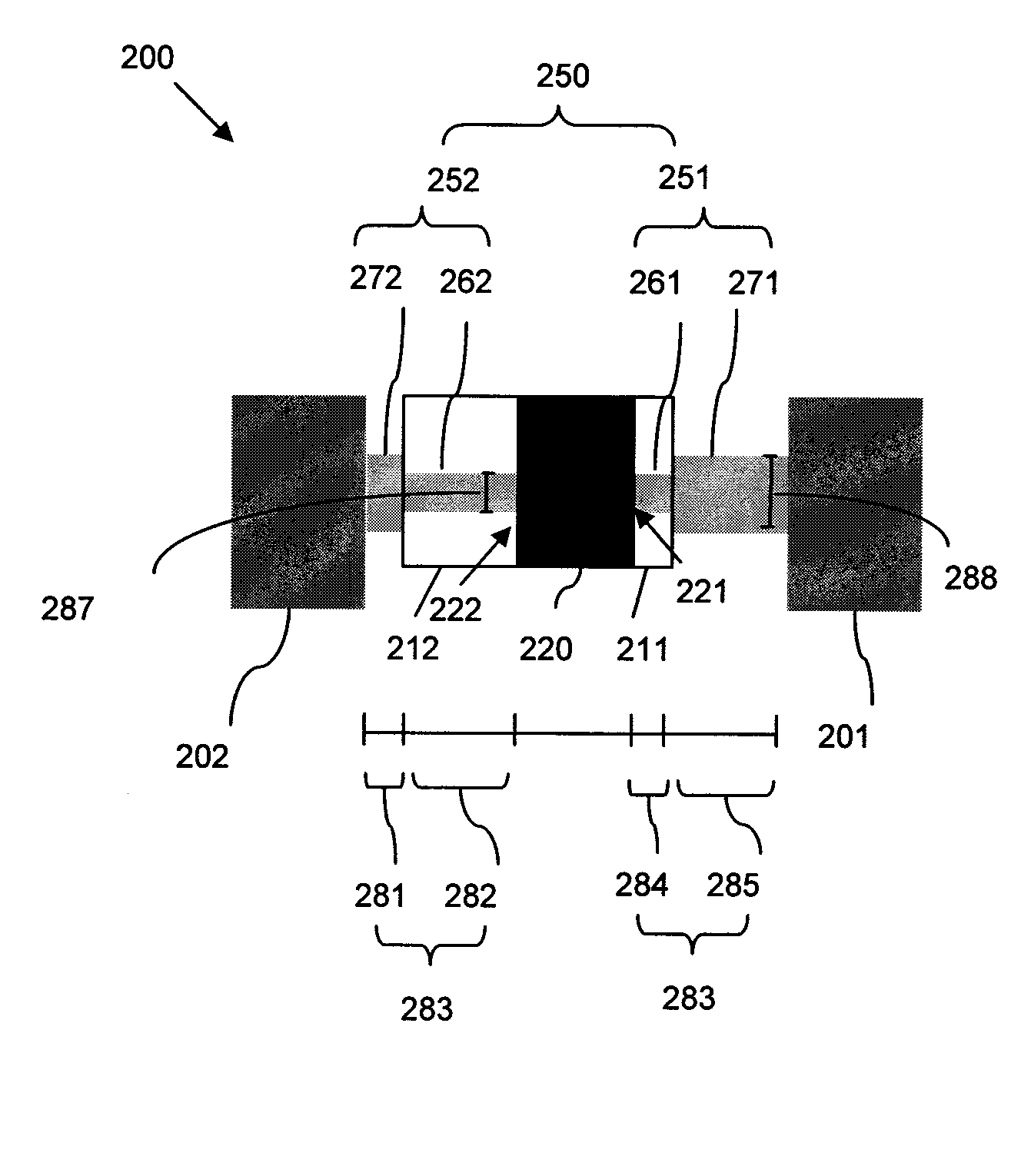
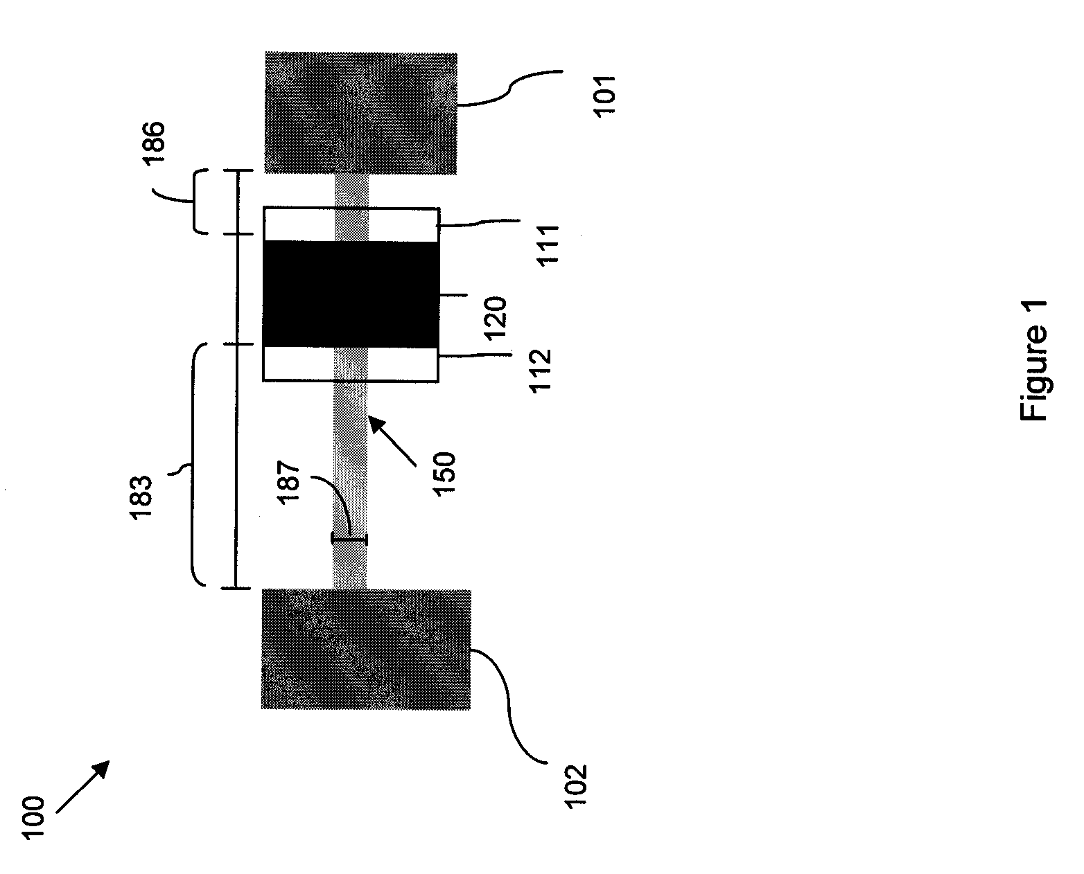
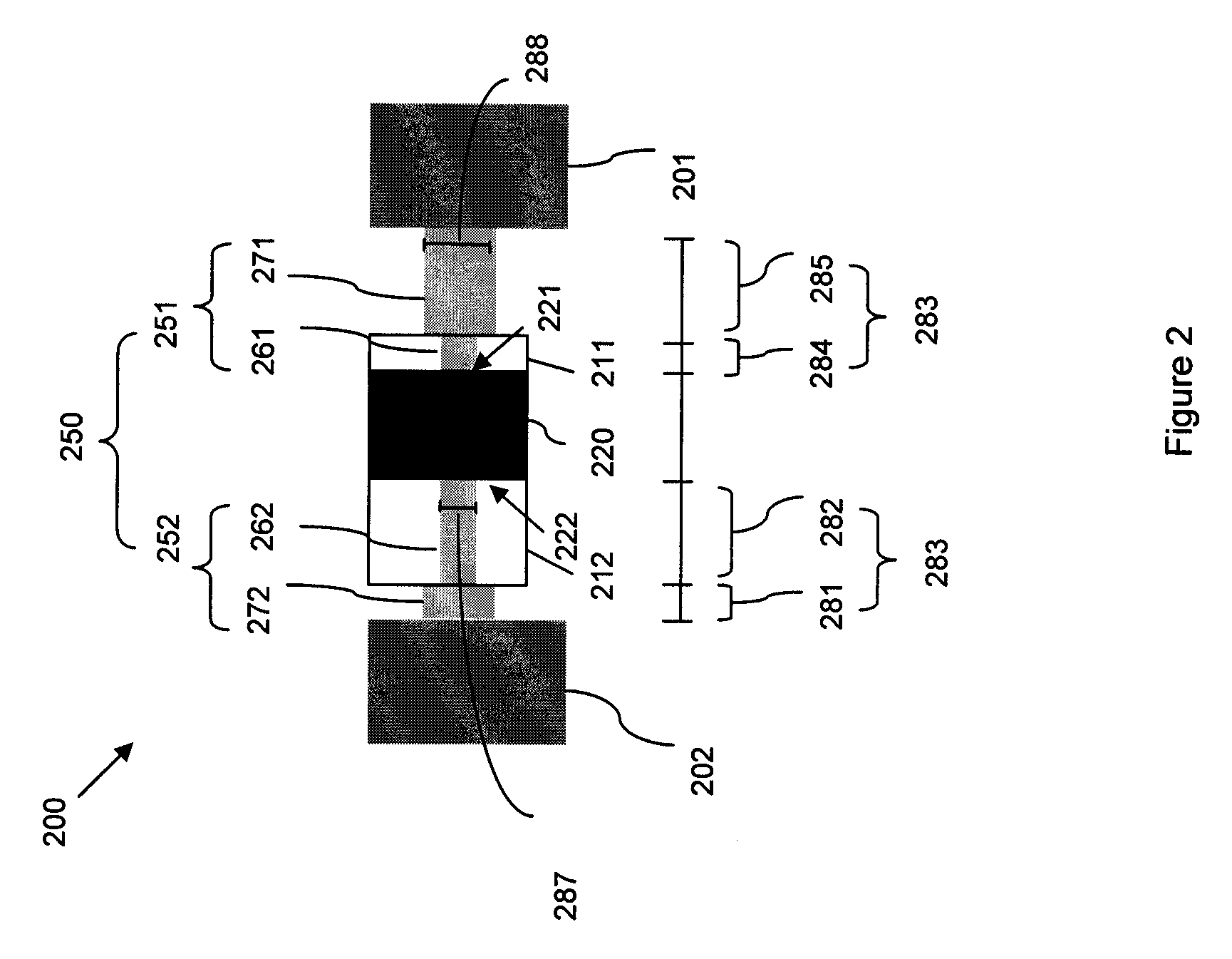
[0034]Disclosed herein are improved fin-type field effect transistor (FinFET) structures and the associated methods of manufacturing the structures. In one embodiment FinFET drive current is optimized by configuring the Fin...


PUM


Abstract

Disclosed herein are improved fin-type field effect transistor (FinFET) structures and the associated methods of manufacturing the structures. In one embodiment FinFET drive current is optimized by configuring the FinFET asymmetrically to decrease fin resistance between the gate and the source region and to decrease capacitance between the gate and the drain region. In another embodiment device destruction at high voltages is prevented by ballasting the FinFET. Specifically, resistance is optimized in the fin between the gate and both the source and drain regions (e.g., by increasing fin length, by blocking source / drain implant from the fin, and by blocking silicide formation on the top surface of the fin) so that the FinFET is operable at a predetermined maximum voltage.

Description

BACKGROUND OF THE INVENTION[0001]1. Field of the Invention[0002]The invention generally relates to fin-type field effect transistors (FinFET), and more particularly, to an improved FinFET structure in which resistance is increased between the gate and either the drain region or both the source and the drain regions in order to lower Miller effect capacitance between the gate and the drain region and to ballast the FinFET, respectively.[0003]2. Description of the Related Art[0004]As transistor design is improved and evolves, the number of different types of transistors continues to increase. A fin-type field effect transistor (FinFET) is a type of transistor that has a fin, containing a channel region and source and drain regions. A double-gated FinFET is a FinFET with first and second gate conductors on either sidewall of the fin. The gate conductors cover the channel region of the fin, whereas the source and drain regions of the fin extend beyond the coverage of the gate conductors...

Claims


Application Information

Patent Timeline
Patent Type & Authority Patents(United States)
IPC IPC(8): H01L29/06
CPCH01L29/66818H01L29/785H01L29/7856
Inventor NOWAK, EDWARD J.
Owner AURIGA INNOVATIONS INC
Why Eureka
Try Eureka