Controllable nanomechanical memory element

a technology of nanomechanical elements and memory elements, applied in static storage, digital storage, instruments, etc., can solve the problems of reducing the power and typically faster devices produced, the transistor elements used in processors face serious obstacles, and the advances will not go on indefinitely, so as to reduce the size of practical elements, increase the density of memory elements, and reduce device power.

Inactive Publication Date: 2008-04-01
TRUSTEES OF BOSTON UNIV
View PDF12 Cites 73 Cited by
  • Summary
  • Abstract
  • Description
  • Claims
  • Application Information

AI Technical Summary

Benefits of technology

[0019]In accordance with an aspect of the present invention, the nanomechanical memory elements may be stimulated according to various techniques. One such technique is magnetomotive stimulation, which relies on large magnetic fields. Other techniques include capacitive, piezoelectric and optical. According to an advantage of the present invention, the nanomechanical device is excited with a modulated AC signal, and resulting motion is detected through changes in voltage. According to another advantage of the present invention, the nanomechanical device is excited with a modulated AC signal, and the resulting motion is detected by measuring interference patterns generated with a laser directed at the nanomechanical device. According to another advantage of the present invention, the nanomechanical device is fabricated from a piezoelectric material and subjected to piezoelectric excitation. The resultant motion is detected by measuring strain-induced voltages between a top and bottom of the nanomechanical element.
[0020]According to another aspect of the present invention, the nanomechanical device may be fabricated in accordance with a number of techniques including semiconductor fabrication techniques. The materials used to fabricate the nanomechanical include but are not limited to silicon on insulator (SOI) materials, silicon nitride (SiN), silicon carbide (SiC), gallium arsenide (GaAs), gallium nitride (GaN), quartz and diamond. In addition, the nanomechanical device structures may be composed of pure metals, bimetallic strips or other heterogeneous material compositions including semiconductor-metal compositions, multiple semiconductor material compositions, and so forth.
[0021]In accordance with another feature of the present invention, the nanomechanical device can be composed of materials that permit the formation of the device with a built in compressive strain. According to this feature of the present invention, the devices are inherently non-linear, and may be driven by very small AC forces or signals, significantly reducing device power.
[0022]In accordance with another aspect of the present invention, the nanomechanical devices can be made to be multi-stable elements where the device possesses more than two distinct states. The introduction of non-linearity into the nanomechanical device permits the creation of multiple distinct amplitude states in a single nanomechanical element.
[0023]According to another aspect of the present invention, several nanomechanical elements, each having different structural characteristics can be provided on a single contact to permit multiple resonance frequencies for an element, addressable through a single contact. The multiple element configuration with a single contact reduces practical element size and / or increases memory element density.
[0024]According to another aspect of the present invention, the nanomechanical element exhibits a hysteretic frequency response, so that the element has a first maximum amplitude with increasing scanning frequency and second maximum amplitude with decreasing scanning frequency. The increasing and decreasing frequency scans define a region of frequencies in which the nanomechanical element is bistable. Excitation at a single frequency within the hysteretic region permits the device to assume one of two distinct amplitude states.

Problems solved by technology

Indeed, with each new semiconducting device generation, smaller, reduced power and typically faster devices are produced.
However, such advances will not go on indefinitely.
Transistor elements used in processors face serious obstacles, including excess heating, power requirements, and tunneling effects.
Volatile memory does not retain state information once power to the memory element is turned off.
Regardless of the form a memory cell takes, present realizations of computer memory face two serious challenges involving scaling and fragility.
As electronic memory elements are made smaller, significant challenges arise with respect to processing individual components.
With regard to magnetic memory elements, packing density is limited by the superparamagnetic limit.
In addition, magnetic hard drives involve platters and read / write heads which are susceptible to impact shock.
However, these types of memory elements with critical dimensions in the micron range have not been able to achieve either the packing densities or read / write speeds that would make them competitive with conventional electro-capacitive or magnetic devices in present commercial settings.
This is a static bistable condition and cannot be easily changed once the device is fabricated.
In the case of mechanical elements that have critical dimensions in the sub-micron range, however, positionally distinct states are a non-optimal solution.
The reduced usefulness of positionally distinct states for elements having sub-micron dimensions detracts from the ability of the elements to achieve competitive read / write speeds and packing densities.
Nanomechanical elements tend to possess features that preclude easy monitoring of their positional states.
This greater sensitivity prevents physical manipulation of such nanomechanical devices, as such forces are often strong enough to cause failure or destruction during manipulation.
Additionally, due to their intrinsically high stiffness, nanomechanical elements often possess very small amplitudes of motion, even when subjected to very large forces.

Method used


Image

  • Controllable nanomechanical memory element
  • Controllable nanomechanical memory element
  • Controllable nanomechanical memory element

Examples


Embodiment Construction

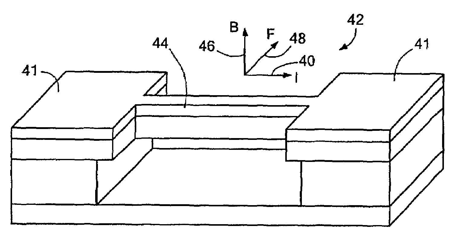
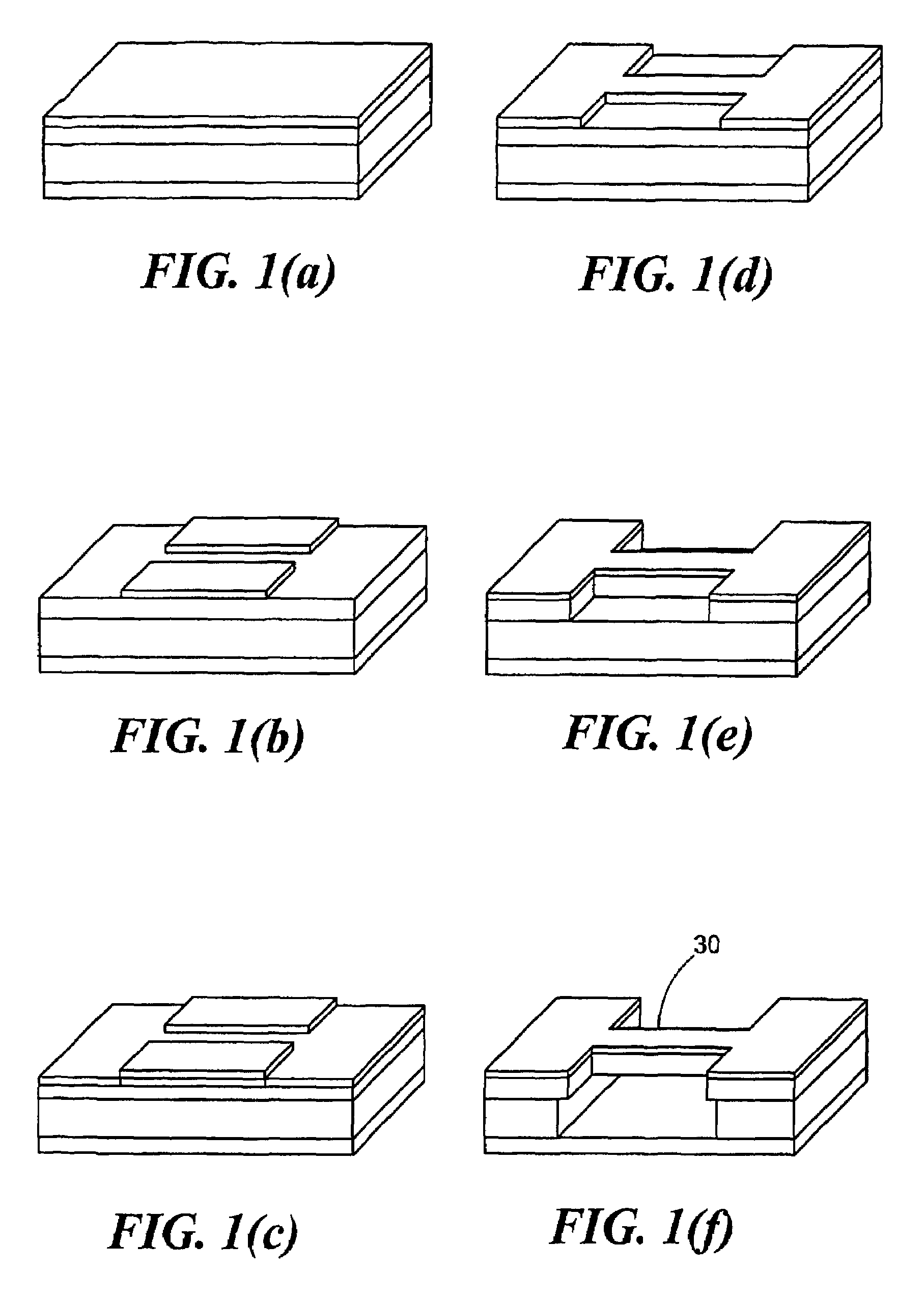
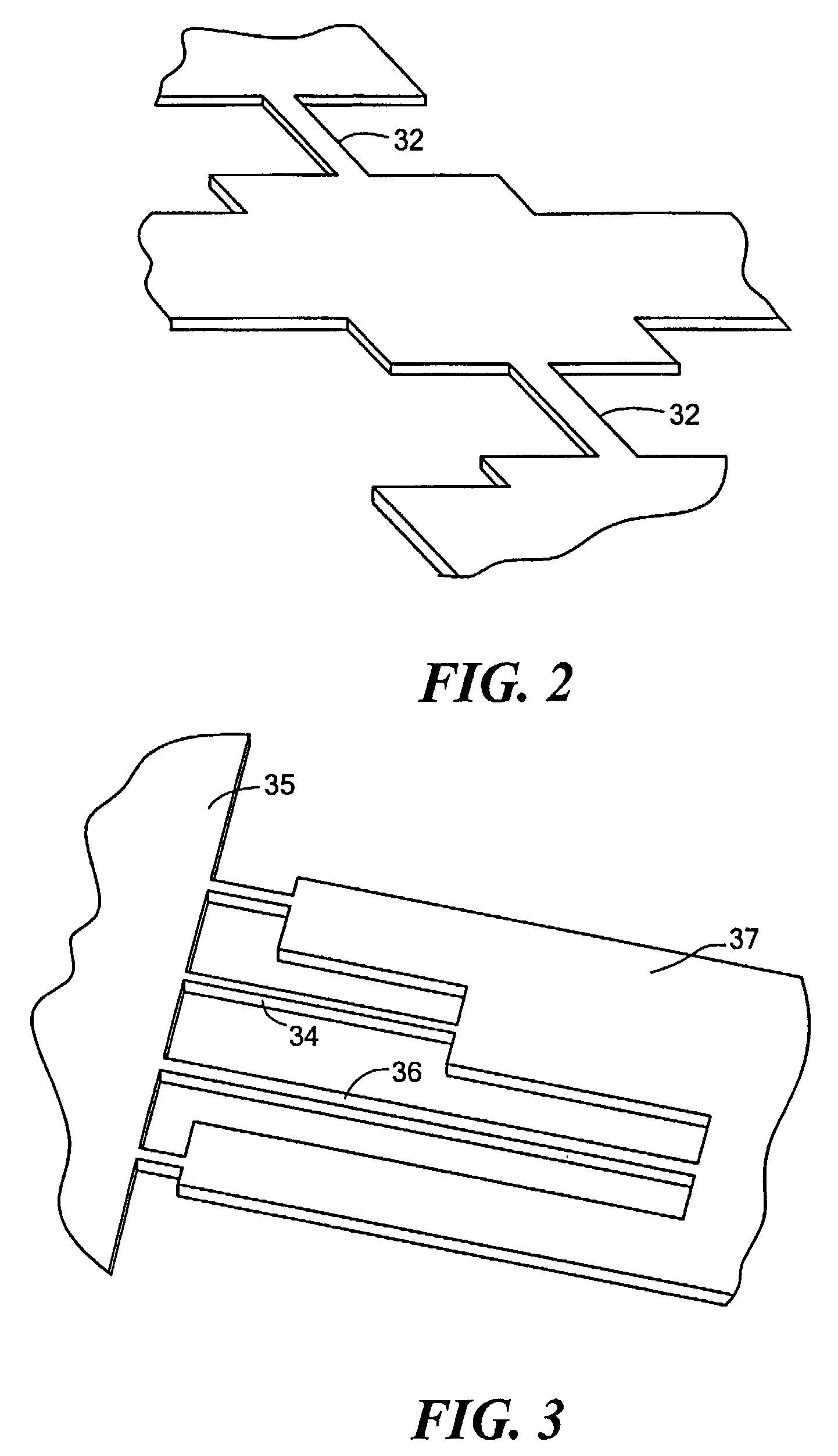
[0055]Referring now to FIGS. 1(a)-1(f), a sequence of fabrication steps for a doubly clamped suspended beam 30 are illustrated. The device is produced with conventional semiconductor fabrication methods beginning with a multilayer structure in FIG. 1(a). The beam pattern is created with lithography techniques in FIG. 1(b), and metalized in FIG. 1(c). FIG. 1(d) illustrates the masking and removal of excess metal and patterning material. FIGS. 1(e) and 1(f) show the removal of material to free beam 30 through anisotropic reactive ion etching (RIE) and isotropic RIE, respectively. Alternatively, it is possible to use a wet etch method for both anisotropic and isotropic etching steps, or any combination of wet etch and RIE. FIG. 2 illustrates a pair of doubly clamped beams 32 that may be formed according to the process illustrated in FIGS. 1(a)-1(f). The two identical individually addressed doubly clamped beams 32 are approximately 8 μm long×300 nm wide×200 nm thick in this exemplary em...


PUM


Abstract

A memory device includes a mechanical element that exhibits distinct bistable states under amplitude modulation. The states are dynamically bistable or multi-stable with the application of a drive signal of a given frequency. The natural resonance of the element in conjunction with a hysteretic effect produces distinct states over a specific frequency range. Devices with multiple elements that respond to different frequency ranges provided on a common contact are formed with improved density. The devices may be excited and read with magnetomotive, capacitive, piezoelectric and / or optical methods. The devices may be planar oriented or out of plane oriented to permit three dimensional memory structures. DC biases may be used to shift frequency responses to permit an alternate method for differentiating states of the element.

Description

CROSS REFERENCE TO RELATED APPLICATIONS[0001]This application claims the priority of U.S. Provisional Application No. 60 / 573,957 filed on May 24, 2004 entitled, CONTROLLABLE NANO MECHANICAL MEMORY ELEMENT, the whole of which is hereby incorporated by reference herein.STATEMENT REGARDING FEDERALLY SPONSORED RESEARCH OR DEVELOPMENT[0002]This invention was made with Government Support under Contract No. ECS-0404206 awarded by the National Science Foundation. The Government has certain rights in the invention.BACKGROUND OF THE INVENTION[0003]1. Field of the Invention[0004]The present invention relates generally to nanomechanical memory devices, and relates more particularly to a nanomechanical device that exhibits discrete states under specific stimuli.[0005]2. Description of Related Art[0006]For many years, semiconducting devices have been used to fabricate memory arrays or storage units. The fabrication of such devices on a micrometer scale has provided a number of attractive advantag...

Claims


Application Information

Patent Timeline
Patent Type & Authority Patents(United States)
IPC IPC(8): G11C13/00
CPCG11C11/56G11C23/00Y10S977/943Y10S977/932
Inventor MOHANTY, PRITIRAJBADZEY, ROBERT L.GAIDARZHY, ALEXEIZOLFAGHARKHANI, GUITI
Owner TRUSTEES OF BOSTON UNIV
Why Eureka
Try Eureka