Integrated passive devices with high Q inductors

a high-q, inductors technology, applied in the direction of inductors, transistors, basic electric elements, etc., can solve the problems of large mutual inductance, inconvenient design, and excessive linear space in a conventional ipd, and achieve the effect of high performance components and less demanding

Inactive Publication Date: 2008-04-08
SYCHIP
View PDF8 Cites 35 Cited by
  • Summary
  • Abstract
  • Description
  • Claims
  • Application Information

AI Technical Summary

Benefits of technology

[0012]A consequence of this new approach is that the structure allows different substrates to be used in the two portions. Thus a silicon IPD substrate may be used for the first portion of the inductor, and a GaAs substrate, for example, may be used for the second portion of the inductor. Other components may be built on the substrates according to the demands needed, i.e. high performance components may be added on the GaAs substrate, and less demanding components located on the silicon substrate.

Problems solved by technology

This results in a large mutual inductance.
Straight conductors, that is, elongated pairs of runners, achieve this goal in principle but consume excessive linear space in a conventional IPD.
In state of the art integrated passive devices some of the design goals are in conflict.
However, each added multiple level in an IPD substrate increases cost.

Method used


Image

  • Integrated passive devices with high Q inductors
  • Integrated passive devices with high Q inductors
  • Integrated passive devices with high Q inductors

Examples


Embodiment Construction

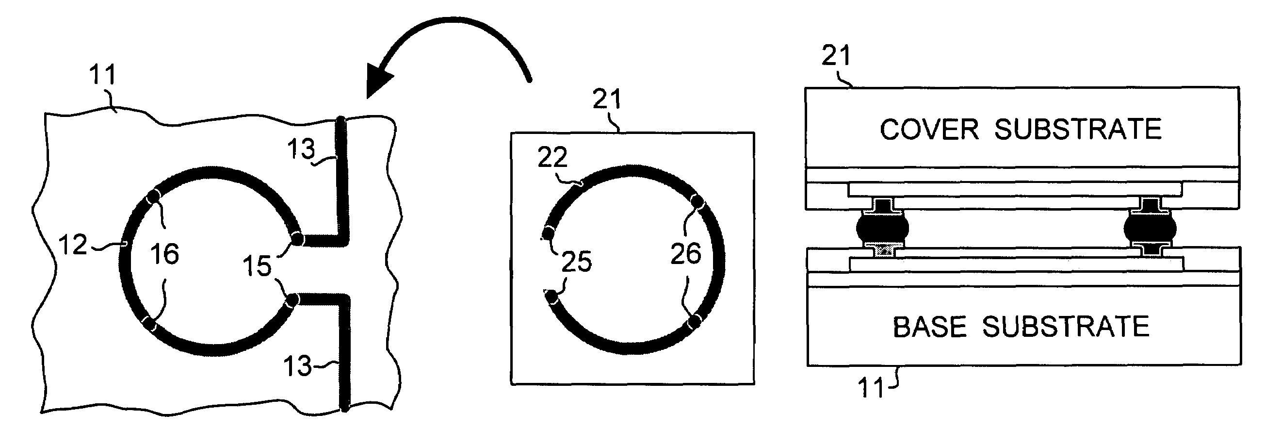
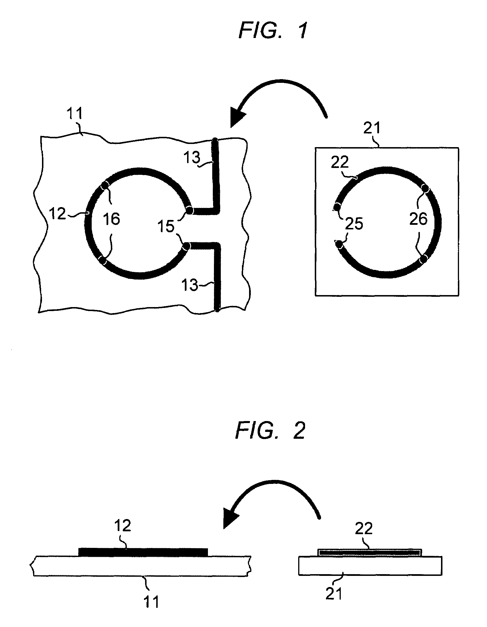
[0020]FIG. 1 is a top view of the base substrate 11 and the cover substrate 21, each carrying half of the inductor structure. In the embodiment shown, the inductor body, comprising elements 12 and 22, is in the pattern of an arc greater than 270 degrees. The inductor body comprises a metal conductor, typically aluminum, copper, or other suitable conductive material. Interconnection runners to the inductor body 12 on the base substrate are shown at 13. Mating interconnections connecting the two halves of the inductor body are shown at 15 and 25. Intermediate interconnections, which are optional, are shown at 16 and 26. The use of intermediate interconnections in a stacked multilevel inductor is discussed in Yin et al., referenced earlier. The two substrates are shown in an elevation view in FIG. 2.

[0021]Substrate 11 is illustrated as a portion of a larger substrate. Typically one or both the base substrate and the cover substrate will have additional circuitry on the substrate. The a...


PUM


Abstract

The specification describes flip bonded dual substrate inductors wherein a portion of the inductor is constructed on a base IPD substrate, a mating portion of the inductor is constructed on a cover (second) substrate. The cover substrate is then flip bonded to the base substrate, thus mating the two portions of the inductor. Using this approach, a two level inductor can be constructed without using a multilevel substrate. Using two two-level substrates yields a four-level flip bonded dual substrate inductor.

Description

FIELD OF THE INVENTION[0001]This invention relates to integrated passive devices (IPDs) and more specifically to improved integrated inductors.BACKGROUND OF THE INVENTION[0002](Portions of the technical material contained in this section may not be prior art.)[0003]State of the art radio-frequency (RF) electrical circuits use large quantities of inductors. Many of these circuits are used in hand held wireless products. Accordingly, miniaturization of passive devices and passive device circuits is an important goal in RF device technology.[0004]Recent advances in passive device technology have produced integrated passive devices (IPDs) wherein inductors, capacitors, and resistors are integrated on a single compact substrate. IPD substrates are large, and preferably made of silicon, but in some cases ceramic. More details on IPD structures and their manufacture can be found in U.S. application Ser. No. 11 / 030,754, filed Jan. 6, 2005, which is incorporated herein by reference.[0005]Des...

Claims


Application Information

Patent Timeline
Patent Type & Authority Patents(United States)
IPC IPC(8): H01L23/48
CPCH01F17/0006H01L28/10H01F2017/002H01F2017/0086H01L27/0641H01L2924/0002H01L2924/00
Inventor DEGANI, YINONCHEN, YINCHAOFAN, YUGAO, CHARLEY CHUNLEISUN, KUNQUANSUN, LIQUO
Owner SYCHIP
Why Eureka
Try Eureka