Method for production of a buried stop zone in a semiconductor component and semiconductor component comprising a buried stop zone

a technology of stop zone and semiconductor component, which is applied in the direction of semiconductor devices, electrical apparatus, transistors, etc., can solve the problems of component damage, current chopping, and small current drop

Inactive Publication Date: 2008-04-22
INFINEON TECH AG
View PDF17 Cites 20 Cited by
  • Summary
  • Abstract
  • Description
  • Claims
  • Application Information

AI Technical Summary

Benefits of technology

[0033]The stop zone does not significantly increase the forward resistance and is advantageous particularly in such components which have a low doping of the second semiconductor zone or the drift zone in order to achieve a good stability toward cosmic radiation.

Problems solved by technology

All of the components mentioned are subject to the problem that current chopping can occur during the turn-off of the component, that is to say during the transition of the component from a current-conducting to a blocking state.
Since the circuitry of such components means that parasitic inductances are unavoidably present, particularly in the leads, and the voltage in these inductances, as is known, is proportional to the derivative of the current, a rapid decrease in the current to very small values effects a high induced voltage that may lead to damage to the component.
Furthermore, the appearance of abrupt current changes may be undesirable for specific applications, for example when using a diode as a freewheeling diode in a semiconductor component.
What is disadvantageous in this case is that the losses increase since, as the thickness of the drift zone increases, the forward resistance also increases.

Method used


Image

  • Method for production of a buried stop zone in a semiconductor component and semiconductor component comprising a buried stop zone
  • Method for production of a buried stop zone in a semiconductor component and semiconductor component comprising a buried stop zone
  • Method for production of a buried stop zone in a semiconductor component and semiconductor component comprising a buried stop zone

Examples


Embodiment Construction

[0047]In the figures, unless specified otherwise, identical reference symbols designate identical parts and regions with the same meaning.

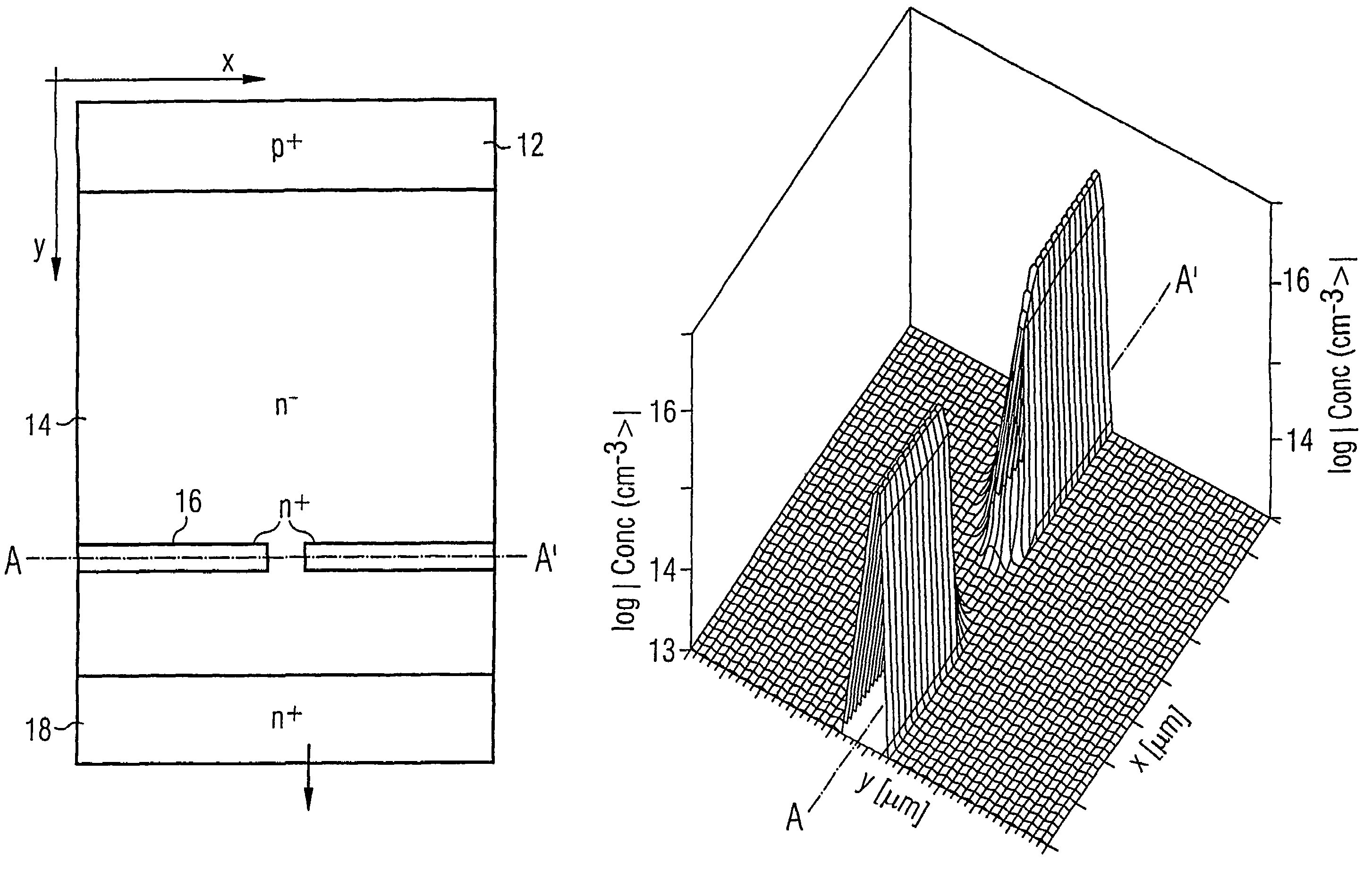
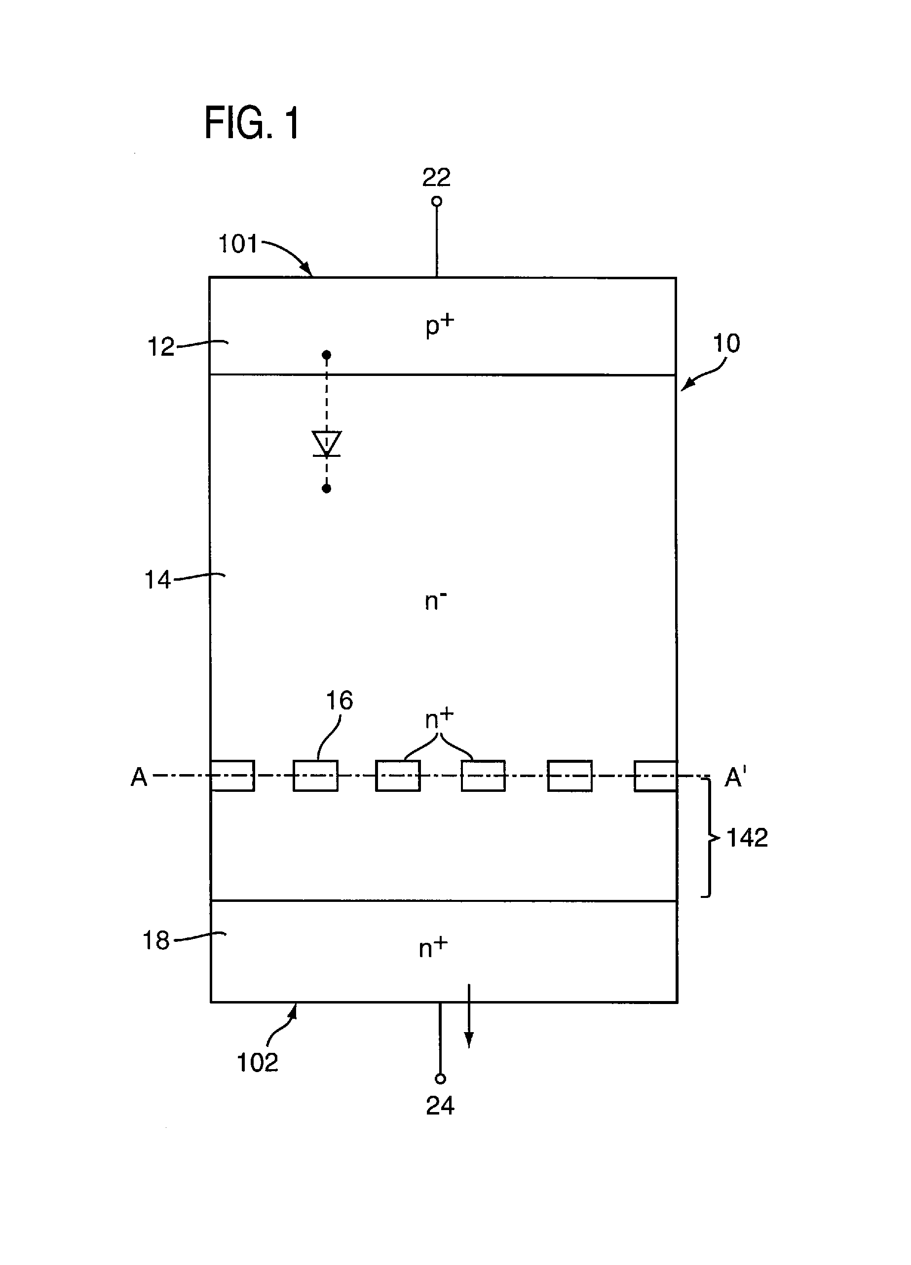
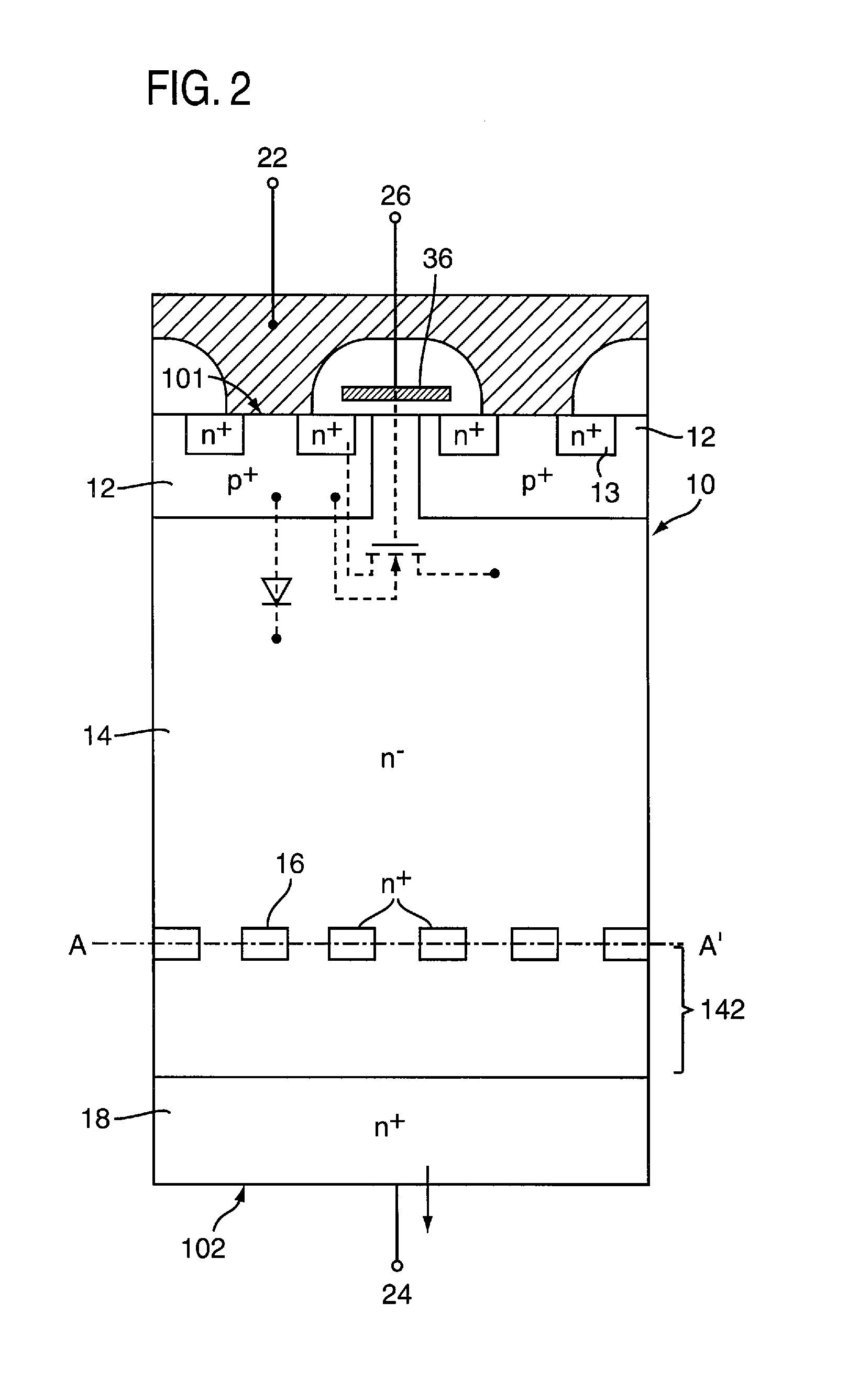
[0048]FIG. 1 shows the detail from a semiconductor body 10 of a vertical semiconductor component according to the invention formed as a diode. The component has a p-doped first semiconductor zone 12, which is arranged in the region of the front side 101 of the semiconductor body 10 and is adjoined by a weakly n-doped second semiconductor zone 14 in the vertical direction. Said second semiconductor zone 14 is adjoined by a heavily n-doped third semiconductor zone 18 in the vertical direction, said third semiconductor zone forming the rear side 102 of the semiconductor body 10.

[0049]According to the invention, a stop zone 16 is present in the second semiconductor zone 14 at a distance from the third semiconductor zone 18, which stop zone is doped more heavily than the remaining region of the second semiconductor zone 14 and is of the same conduction...


PUM


Abstract

A method for the production of a stop zone in a doped zone of a semiconductor body having a first side and a second side, comprises the following method steps:applying a mask having cutouts to one of the sides of the semiconductor body,irradiating the side having the mask with proton radiation,carrying out a heat treatment method in order to produce hydrogen-induced donors in the semiconductor body.

Description

CROSS REFERENCE TO RELATED APPLICATION[0001]This application is a continuation of copending International Application No. PCT / EP03 / 09494 filed Aug. 27, 2003 which designates the United States, and claims priority to German application no. 102 43 758.0 filed Sep. 20, 2002.TECHNICAL FIELD OF THE INVENTION[0002]The present invention relates to a semiconductor component, in particular a vertical power semiconductor component, having a doped first semiconductor zone of a first conduction type, a doped second semiconductor zone of a second conduction type, which adjoins the first semiconductor zone and is doped more weakly than the first semiconductor zone, a doped third semiconductor zone, which adjoins the second semiconductor zone and is doped more heavily than the second semiconductor zone.BACKGROUND OF THE INVENTION[0003]A semiconductor structure of this type is present both in vertical diodes and vertical transistors and in thyristors, the second, more weakly doped semiconductor zon...

Claims


Application Information

Patent Timeline
Patent Type & Authority Patents(United States)
IPC IPC(8): H01L31/0248H01L29/08H01L29/32H01L29/739H01L29/78H01L29/861H01L29/868
CPCH01L29/868H01L21/263H01L29/7395H01L29/7802H01L29/861H01L29/0847H01L29/32H01L29/0878H01L29/167H01L29/36H01L29/66136H01L29/66333H01L29/66712
Inventor BARTHELMESS, REINERMAUDER, ANTONNIEDERNOSTHEIDE, FRANZ-JOSEFSCHULZE, HANS-JOACHIM
Owner INFINEON TECH AG
Why Eureka
Try Eureka