Applied voltage control circuit for voltage controlled oscillation circuit

a voltage control circuit and voltage control technology, applied in the direction of oscillation generators, pulse automatic control, generator starters, etc., can solve the problem of not meeting the minimum allowable value to recognize the “h” level of the transmission gate, and the “h” level of the general purpose port is long

Inactive Publication Date: 2008-05-06
PANASONIC CORP
View PDF5 Cites 0 Cited by
  • Summary
  • Abstract
  • Description
  • Claims
  • Application Information

AI Technical Summary

Benefits of technology

[0009]A main object of the present invention is as follows. It is able to supply a power-supply voltage higher than a voltage level of a control signal applied to a general purpose port, which can be controlled by an external microcomputer or LSI, based on an amplifying operation of a transistor at starting a power supply even though the voltage level of the control signal does not satisfy a minimum allowable value to recognize “H” level of a transmission gate. As a result, a length of time required for stabilizing oscillation of a quartz resonator in a voltage controlled oscillation circuit is reduced, and a polarity of the general purpose port externally controlled is reversed after the oscillation is stabilized, so that the voltage switched to the control through a voltage control terminal to keep the stabilized oscillation continuously.
[0017]According to the foregoing configuration, even when the voltage level of the control signal applied to the general purpose terminal when the power supply is turned on does not satisfy the minimum allowance level for recognizing the “H” level of the transmission gate, the amplifying operation of the NPN transistor is utilized so that the voltage of the NPN transistor on the collector side is increased to reach such a voltage level that recognizes the “H” level at the transmission gates, which allows the transmission gates to be switched. Then, the first transmission gate is conducted when the power supply is turned on so that the power-supply voltage higher than the voltage level of the control signal is supplied. Thereby, the length of time required for the oscillation of the quartz resonator in the voltage controlled oscillation circuit to be stabilized is reduced, and the polarity of the general purpose terminal externally controlled is inverted after the oscillation is stabilized. As a result, the control operation shifts to the control through the voltage control terminal, and the stabilized oscillation can be continuously obtained.
[0027]According to the foregoing configuration, even when the voltage level of the control signal applied to the general purpose terminal when the power supply is turned on does not satisfy the minimum allowance level for recognizing the “H” level of the transmission gate, the amplifying operations of the first and second NPN transistors are utilized so that the voltage of the second NPN transistor on the collector side is increased to reach such a voltage level that recognizes the “H” level at the transmission gates, which allows the transmission gates to be switched. Then, the first transmission gate is conducted when the power supply is turned on so that the power-supply voltage higher than the voltage level of the control signal is supplied. Thereby, the length of time required for the oscillation of the quartz resonator in the voltage controlled oscillation circuit to be stabilized is reduced, and the polarity of the general purpose terminal externally controlled is inverted after the oscillation is stabilized. As a result, the control operation shifts to the control through the voltage control terminal, and the stabilized oscillation can be continuously obtained. Further, because the first and second NMOS transistors and the PNP transistor are provided, there is a sufficient amount of time for the first transmission gate to be conducted with respect to a timing of starting the oscillation of the quartz resonator, and the power-supply voltage higher than the voltage level of the control signal can be applied. As a result, the oscillation can be further stabilized.
[0035]According to the foregoing configuration, when the state where the first transmission gate is conducted is switched to the state where the second transmission gate is conducted, the first and second transmission gates are simultaneously conducted due to a delay time in the inverter, an internal wiring delay or the like, and the power-supply voltage may be applied to a control port of the LSI or external microcomputer via the both transmission gates. Therefore, the pull-up resistance is additionally provided as described so that a period of the transition from the “H” level to the “L” level is extended to be longer than the delay time so that a period when the transmission gates are simultaneously conducted is not generated. Thereby, the control port of the LSI or external microcomputer can be prevented from any overload applied thereto.

Problems solved by technology

As a result, a long time is required to start the oscillation.
As a first problem, there causes a possibility that “H” level of a general purpose port, which can be controlled by the LSI or external microcomputer, may not satisfy a minimum allowable value to recognize the “H” level of the transmission gate.
As a result, the transmission gate cannot be conducted after the oscillation is stabilized, which makes the control through the voltage control terminal impossible.
As a second problem, when gates of the PMOS transistor and the transmission gate are switched immediately after the power supply is turned on and after the oscillation is stabilized, a period when the PMOS transistor and the transmission gate are simultaneously conducted is generated due to influences such as a delay of the inverter resulting from the inversion of the signal.
As a result, the power-supply voltage is applied to the voltage control terminal, which is likely to cause an overload to a control port of the LSI or external microcomputer.

Method used


Image

  • Applied voltage control circuit for voltage controlled oscillation circuit
  • Applied voltage control circuit for voltage controlled oscillation circuit
  • Applied voltage control circuit for voltage controlled oscillation circuit

Examples


first preferred embodiment

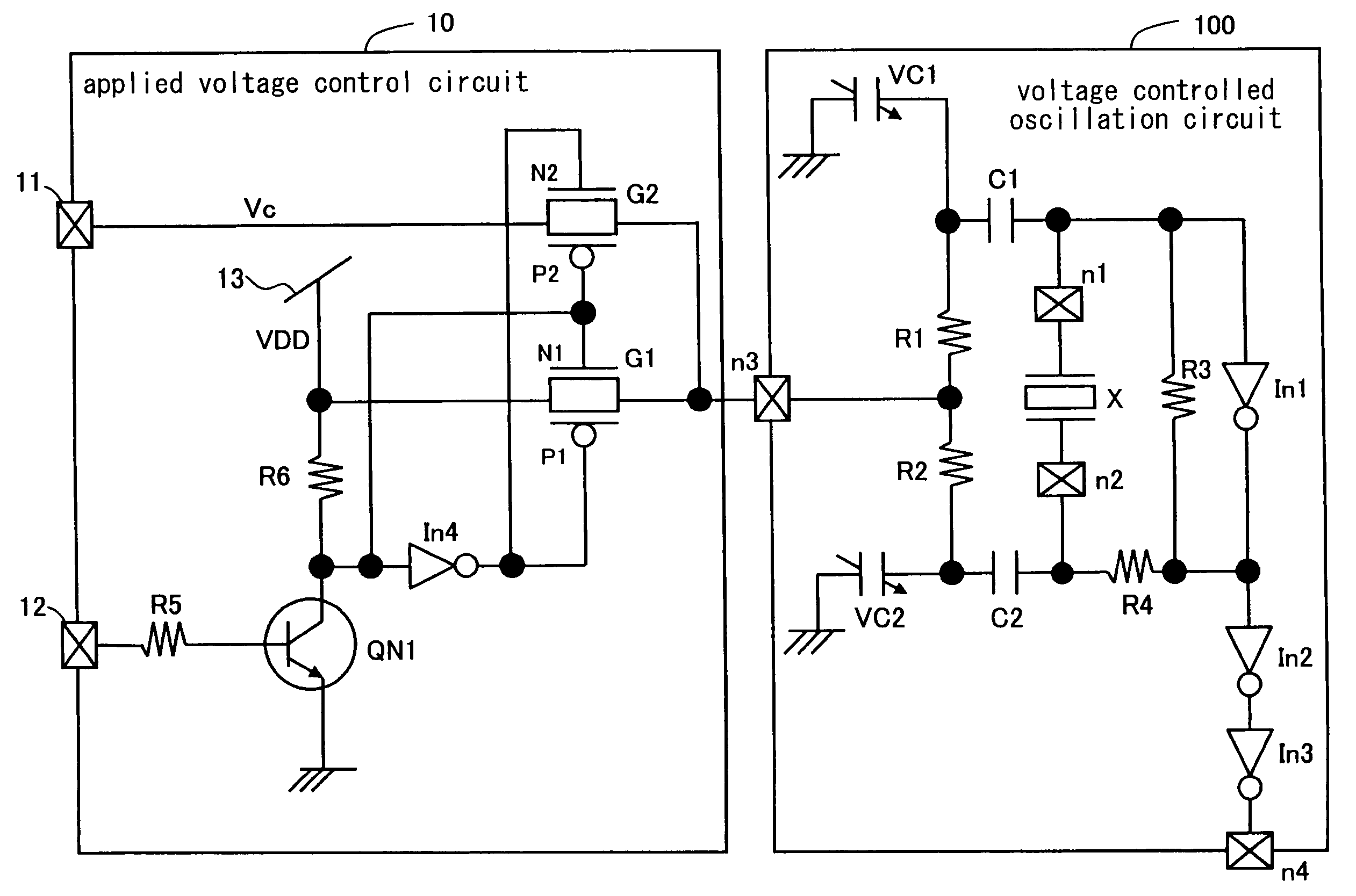
[0069]FIG. 1 is a circuit diagram illustrating configurations of an applied voltage control circuit 10 for a voltage controlled oscillation circuit and a voltage controlled oscillation circuit 100 according to a first preferred embodiment of the present invention.

[0070]The voltage controlled oscillation circuit 100, which is configured in a manner similar to that of the conventional technology shown in FIG. 10, is not described below again.

[0071]The applied voltage control circuit 10 comprises, as main components thereof, a first transmission gate G1, a second transmission gate G2, and an NPN transistor QN1 for switching an applied voltage. The first transmission gate G1 determines application / disconnection of a power-supply voltage VDD with respect to a control input terminal n3 of the voltage controlled oscillation circuit 100. The second transmission gate G2 determines application / disconnection of a voltage level Vc of a control signal from a voltage control terminal 11 with resp...

second preferred embodiment

[0079]A second preferred embodiment of the present invention realizes an operation achieving a higher speed in comparison to the first preferred embodiment.

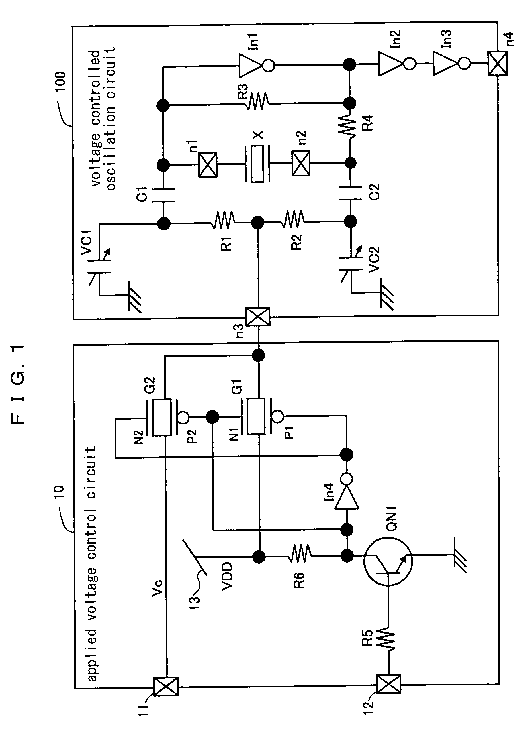
[0080]FIG. 2 is a circuit diagram illustrating configurations of an applied voltage control circuit 20 for a voltage controlled oscillation circuit and a voltage controlled oscillation circuit 100 according to the second preferred embodiment.

[0081]In the present embodiment, the inverter In4 according to the first preferred embodiment is omitted, and an NPN transistor QN2, a PNP transistor QP1 and an inverter In5 are additionally provided.

[0082]A base of the NPN transistor QN2 is connected to a collector of the NPN transistor QN1 via a resistance R7, an emitter thereof is grounded, and a collector thereof is connected to a base of the PNP transistor QP1 via a resistance R8. An emitter of the PNP transistor QP1 is connected to the power-supply voltage terminal 13 to which the power-supply voltage VDD is applied, and a collector the...

third preferred embodiment

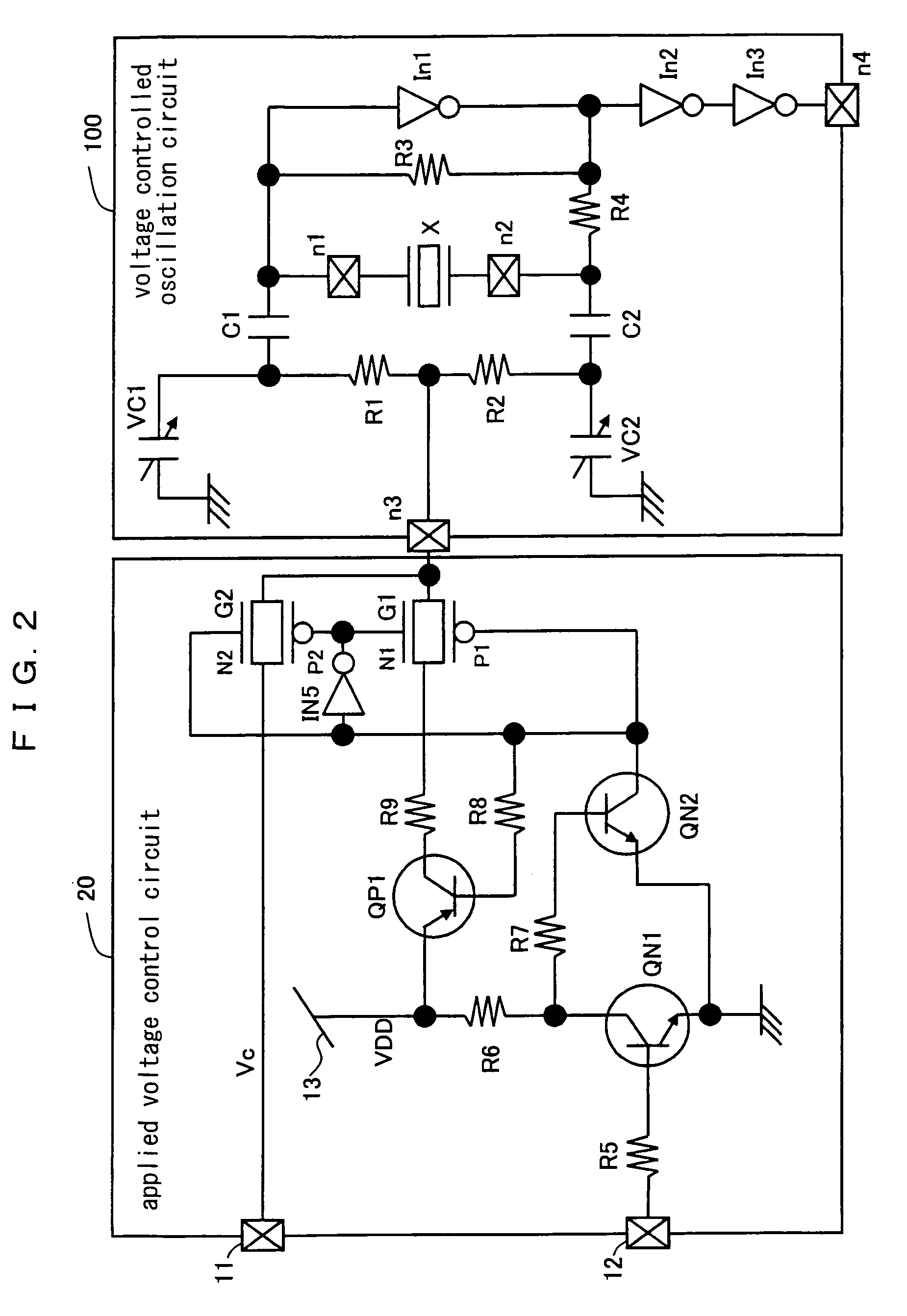
[0090]FIG. 4 is a circuit diagram illustrating configurations of an applied voltage control circuit 30 for a voltage controlled oscillation circuit and a voltage controlled oscillation circuit 100 according to a third preferred embodiment of the present invention.

[0091]The first transmission gate G1 is inserted between the control input terminal n3 of the voltage controlled oscillation circuit 100 and the power-supply voltage terminal 13 to which the power-supply VDD is supplied. The second transmission gate G2 is inserted between the control input terminal n3 and the voltage control terminal 11 to which the voltage level Vc of the control signal is applied. The general purpose terminal 12 for external control is connected to the gate of the PMOS transistor P1 of the first transmission gate G1 and the gate of the NMOS transistor N2 of the second transmission gate G2. The general purpose terminal 12 is further connected to the gate of the NMOS transistor N1 of the first transmission ...


PUM


Abstract

When a power supply is turned on, an NPN transistor is disconnected, a first transmission gate is conducted, a second transmission gate is disconnected, and a power-supply voltage is applied to a control input terminal of a voltage controlled oscillation circuit via the first transmission gate. After oscillation of a quartz resonator is stabilized, the NPN transistor is switched to the conducted state by a control signal applied to a general purpose terminal so that the first transmission gate is switched to the disconnected state, and the second transmission gate is switched to the conducted state. Then, a voltage of the voltage control terminal is applied to the control input terminal of the voltage controlled oscillation circuit via the second transmission gate.

Description

FIELD OF THE INVENTION[0001]The present invention relates to an applied voltage control circuit for a voltage controlled oscillation circuit (VCO), and is effectively applied to an applied voltage control circuit for a voltage controlled oscillation circuit which can be controlled by an external microcomputer, LSI or the like. Further, the present invention can also be applied to circuits in general for switching to and from a voltage while a power supply is turned and a voltage after the power supply is turned on.BACKGROUND OF THE INVENTION[0002]A conventional voltage controlled oscillation circuit 100 shown in FIG. 10 comprises a quartz resonator X connected to between two terminals n1 and n2, a capacitor C1 and a varicap (voltage variable capacitance diode) VC1 serially connected to between the terminal n1 and ground GND, a capacitor C2 and a varicap VC2 serially connected to between the terminal n2 and the ground GND, resistance elements R1 and R2 serially connected to between a...

Claims


Application Information

Patent Timeline
Patent Type & Authority Patents(United States)
IPC IPC(8): H03B5/32
CPCH03B5/06H03B5/366H03L3/00
Inventor MATSUMOTO, KENICHI
Owner PANASONIC CORP
Why Eureka
Try Eureka