Combined nanoimprinting and photolithography for micro and nano devices fabrication

a nano-scale patterning and nano-technology, applied in the field of nano-scale patterning for nano-scale structures, can solve the problems of inability to achieve the effect of high-throughput and significant practical valu

Active Publication Date: 2008-05-20
RGT UNIV OF MICHIGAN
View PDF0 Cites 80 Cited by
  • Summary
  • Abstract
  • Description
  • Claims
  • Application Information

AI Technical Summary

Benefits of technology

[0005]Nanoimprint lithography (NIL) is a nano-scale lithography technique where a surface relief pattern on a hard mold is physically imprinted into a thermal plastic polymer film at elevated temperature and pressure. Nanoimprint lithography has attracted more and more attention in both research and commercial applications due to its potential application in nano-scale patterning. It is often desirable because of its sub-10 nm resolution and simple equipment setup requirements. Nanoimprint lithography is further a relatively simple process that has high throughput, thus enabling low-cost, large-scale patterning of nano-structures.
[0008]The present invention combines the processing steps of nanoimprint lithography and photolithography to provide a new technique that provides many new advantages. That is, the present invention enables patterning of both large-scale and sub-micron size structures in a single step. With many advantages, the present invention may be used in the fabrication of a wide range of nano-scale electronic, photonic, and biological devices where patterns of various sizes and densities are needed.

Problems solved by technology

Although nanoimprint lithography has proved to be very successful in nano-patterning, especially in replicating nano-scale features with uniform sizes, it still suffers from several limitations as a flexible lithographic technique.
Thus, patterns with large features are much more difficult to imprint than smaller features (also known as nano-patterns).
Furthermore, defects or pattern failures in the form of incomplete pattern transfer can occur due to the high viscosity of the polymer melt and the mold pattern complexity.
In most cases, the cost of these next generation photolithography systems is prohibitive, except for large-scale production runs.

Method used


Image

  • Combined nanoimprinting and photolithography for micro and nano devices fabrication
  • Combined nanoimprinting and photolithography for micro and nano devices fabrication
  • Combined nanoimprinting and photolithography for micro and nano devices fabrication

Examples


first embodiment

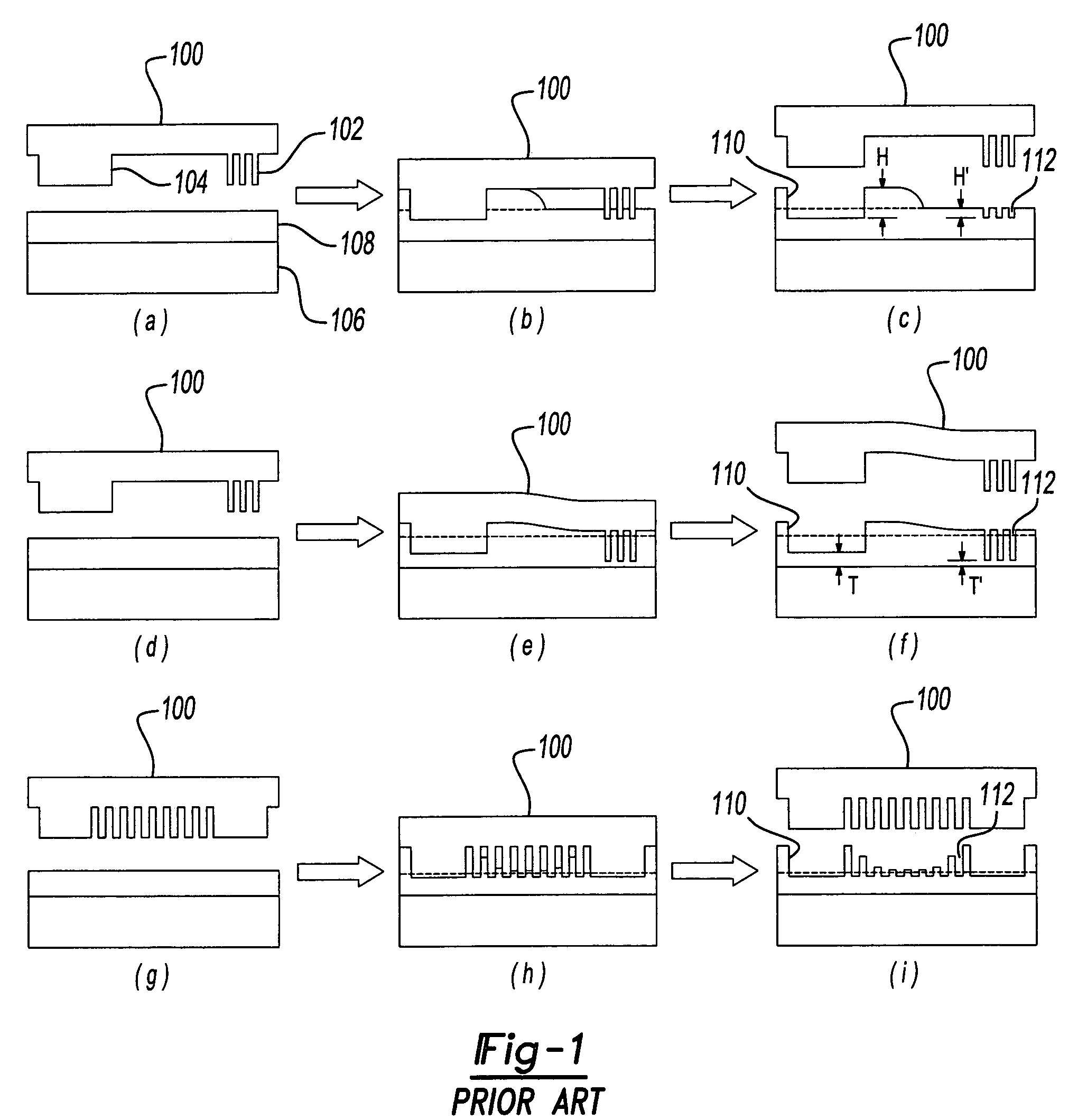
[0040]Therefore, according to the present invention, a novel method of combined nanoimprint and photolithography is provided that integrates the benefits of nanoimprinting with the benefits of photolithography to achieve new micro and nano fabrication capability not otherwise possible using the techniques individually.

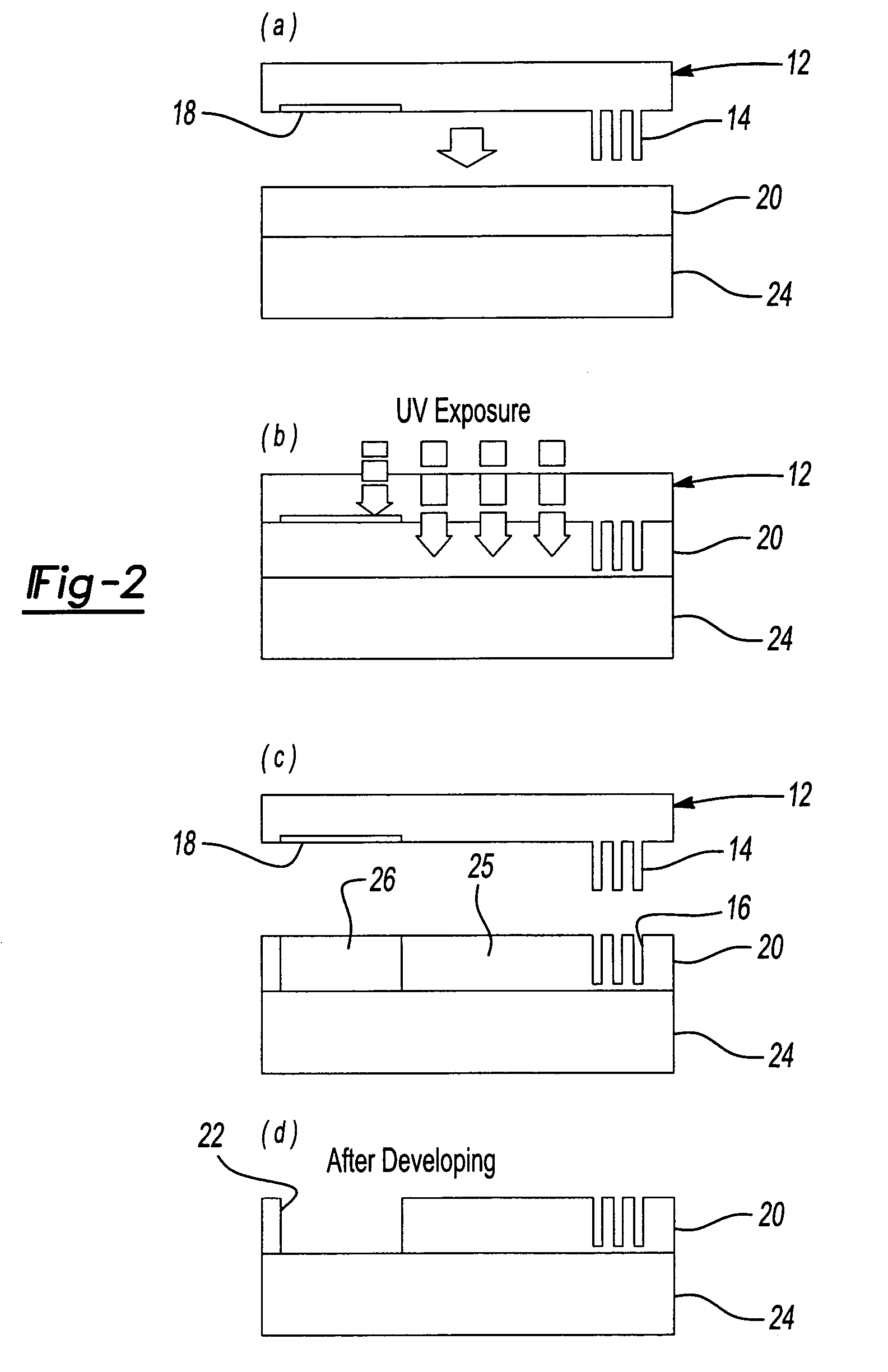
[0041]As best seen in FIGS. 2(a)-(d), the method according to the present invention is illustrated. The present invention employs a hybrid mold configuration, generally indicated at 12, which acts as both a nanoimprint lithography mold and a photolithography mask—an example of hybrid mold 12 is illustrated at FIG. 2(a). Hybrid mold 12 is preferably made of an ultraviolet (UV) transparent material, such as fused silica. Protrusions 14 are formed on hybrid mold 12 for physically imprinting nano-scale features 16 within a resist layer 20 on a substrate 24. Hybrid mold 12 further includes mask members 18, in the form of metal pads, embedded therein to serve as ultraviolet ...

second embodiment

[0048]According to the present invention, yet another new method of combined nanoimprint and photolithography is provided wherein a metal layer is placed on an end of the mold protrusion feature, which eliminates the separate residual removal step in nanoimprint lithography.

[0049]According to the present embodiment as illustrated in FIGS. 5(a)-(d), hybrid mold 12 is modified, generally designated as hybrid mold 12′, such that it includes a light-blocking metal layer 50, such as nickel, disposed at an end of nano-scale protrusions 14. Metal layer 50, similar to metal layer 18, acts as an embedded photomask and prevents ultraviolet radiation from penetrating into portions of resist layer 20 (specifically, a residual layer of resist disposed at a lowermost portion of the feature on top of substrate 24).

[0050]More particularly, hybrid mold 12′ is first imprinted into resist layer 20, such as a negative tone UV resist (see FIG. 5(a)). The entire assembly is then flood-exposed with ultrav...


PUM

PropertyMeasurementUnit
aspect ratioaaaaaaaaaa
sizeaaaaaaaaaa
heightaaaaaaaaaa

Abstract

A method of fabricating a device including imprinting a mold having a protrusion against a substrate having a resist layer such that the protrusion engages the resist layer. The mold further has a mask member positioned generally adjacent the resist layer. Radiation energy is then transmitted through the mold and into the resist layer; however, the mask member substantially prevents transmission of the radiation energy therethrough, thereby defining an unexposed area in the resist layer. Once the mold is removed from the substrate, which consequently forms a first feature from nanoimprinting, the unexposed area of resist layer is removed through dissolving in a developer solution.

Description

CROSS-REFERENCE TO RELATED APPLICATIONS[0001]This application claims the benefit of U.S. Provisional Application No. 60 / 447,116, filed on Feb. 13, 2003. The disclosure of the above application is incorporated herein by reference.STATEMENT OF GOVERNMENTAL SUPPORT[0002]This invention was made with Government support under Grant No. N00014-02-1-0899 awarded by the Office of Naval Research and Grant No. N66001-02-C-8039 awarded by Defense Advanced Research Projects Agency (DARPA). The government has certain rights in this invention.FIELD OF THE INVENTION[0003]The present invention generally relates to the fabrication of nano and microstructures and, more particularly, relates to nano-scale patterning for nano and microstructures as well as potential applications.BACKGROUND AND SUMMARY OF THE INVENTION[0004]Nano-patterning is an essential part of nanotechnology research and is used to fabricate nanostructures to harness their unique properties. However, in order for nano-device and nanos...

Claims


Application Information

Patent Timeline
Patent Type & Authority Patents(United States)
IPC IPC(8): G03C5/00G03F
CPCB82Y10/00B82Y40/00G03F1/14G03F7/0002G03F1/50
Inventor GUO, LINGJIE J.CHENG, XING
Owner RGT UNIV OF MICHIGAN
Why Eureka
Try Eureka