Enhancement electrode configuration for electrically controlled light modulators

a technology of light modulator and enhanced electrode, which is applied in the direction of active addressable light modulator, instruments, optics, etc., can solve the problems of impairing the light modulation capability of the device, the difficulty of producing desired profiles, etc., to facilitate enhanced active deformation of viscoelastic material, shorten the response time, and increase the diffraction efficiency of the light modulator cells

Inactive Publication Date: 2008-05-20
NOKIA CORP
View PDF8 Cites 86 Cited by
  • Summary
  • Abstract
  • Description
  • Claims
  • Application Information

AI Technical Summary

Benefits of technology

[0011]The main purpose of the present invention is to present a novel electrode configuration for light modulator cells based on the use of dielectric and viscoelastic materials to facilitate enhanced and active deformation of viscoelastic material in order to, among other things, increase the diffraction efficiency of the light modulator cells, shorten the response time required to switch a cell (pixel) or corresponding primary optical unit between on and off states, and to reduce the voltage levels required for a defined diffraction amplitude, that is for a certain height of a gel relief. Therefore, the current invention aims to the manufacturing of light modulators with better optical contrast, higher switching speed and smaller power consumption than what can be provided by devices of prior art. The invention also allows the use of softer polymers once more increasing the diffraction amplitude of the gel relief with the named advantages.
[0012]The basic idea of the invention is to utilize active fieldshaping enhancement electrode structure located in the proximity and in addition to the signal electrode structure of a cell in order to affect the electric field between the signal electrode structure and the support electrode structure and through the viscoelastic layer in a manner that the deformation amplitude of the viscoelastic layer in the cell is increased.
[0022]enhancement signal means for applying enhancement signal voltage between the enhancement electrode structure and the signal electrode structure in order to locally concentrate the electric field passing through the two deformable dielectric layers and therefore arranged to enhance the amplitude of the deformation of the viscoelastic gel layer.
[0029]enhancement signal means for applying enhancement signal voltage between the enhancement electrode structure and the signal electrode structure in order to locally concentrate the electric field passing through the two deformable dielectric layers and therefore arranged to enhance the amplitude of the deformation of the viscoelastic gel layer.

Problems solved by technology

The major shortcomings of the light modulators, like the display panels described in WO 01 / 48531, which are based on electrically controlled deformation of dielectric and viscoelastic materials may be associated with the practical difficulties in producing desired profiles for the gel reliefs.
This further impairs the light modulating capabilities of the devices, for example the capabilities of individual pixels or cells.

Method used


Image

  • Enhancement electrode configuration for electrically controlled light modulators
  • Enhancement electrode configuration for electrically controlled light modulators
  • Enhancement electrode configuration for electrically controlled light modulators

Examples


Embodiment Construction

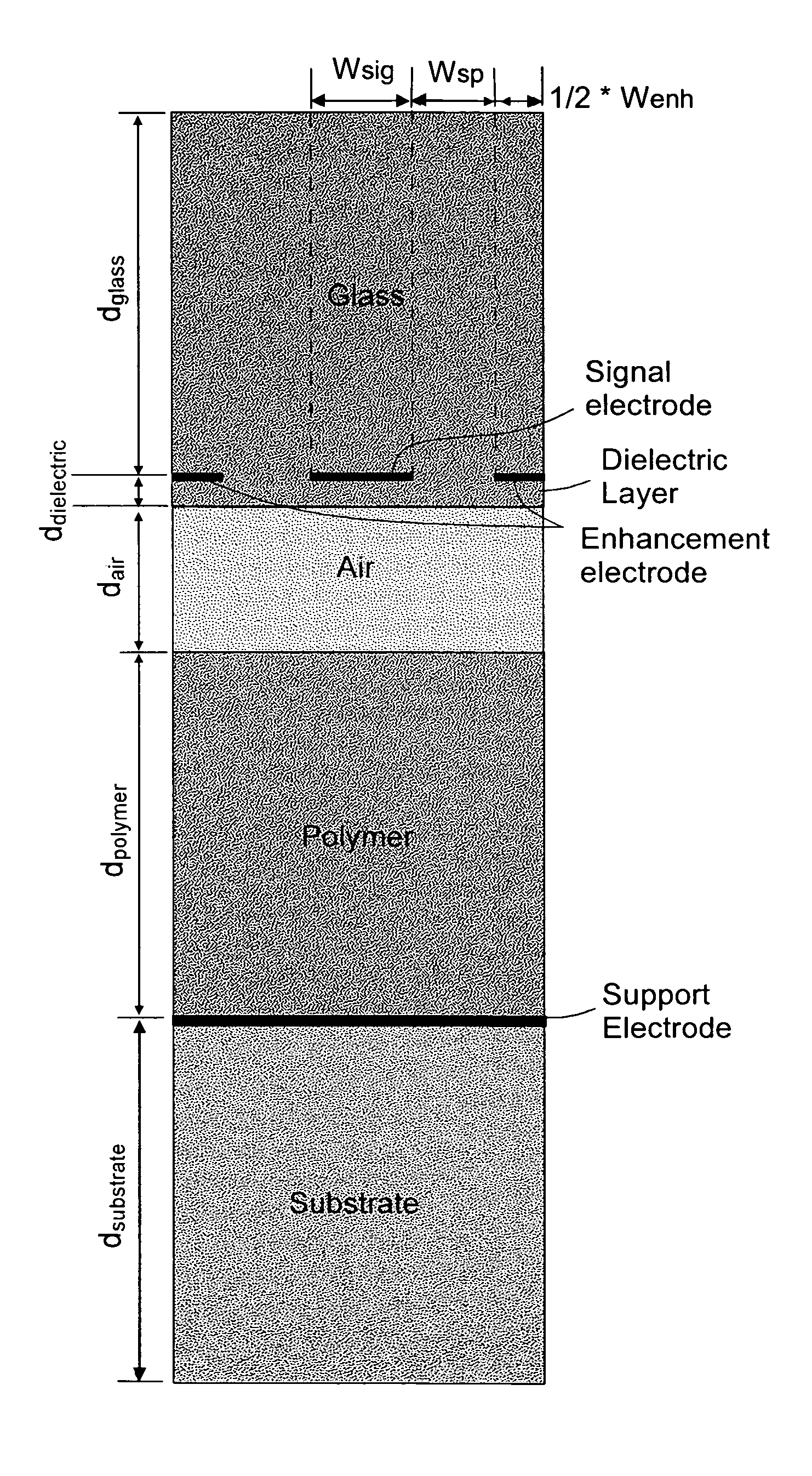
[0043]In the following, the enhancement electrode configurations according to the invention are described in more detail and their benefits compared to the prior art solutions are pointed out using selected simulation results.

[0044]It should be noted that when the invention is applied to display devices, the concept of a cell corresponds closely to a single pixel of a display. However, the invention is not limited to display devices, but can be applied broadly also to other type of light modulators. Therefore, the term cell is mainly used in the following description.

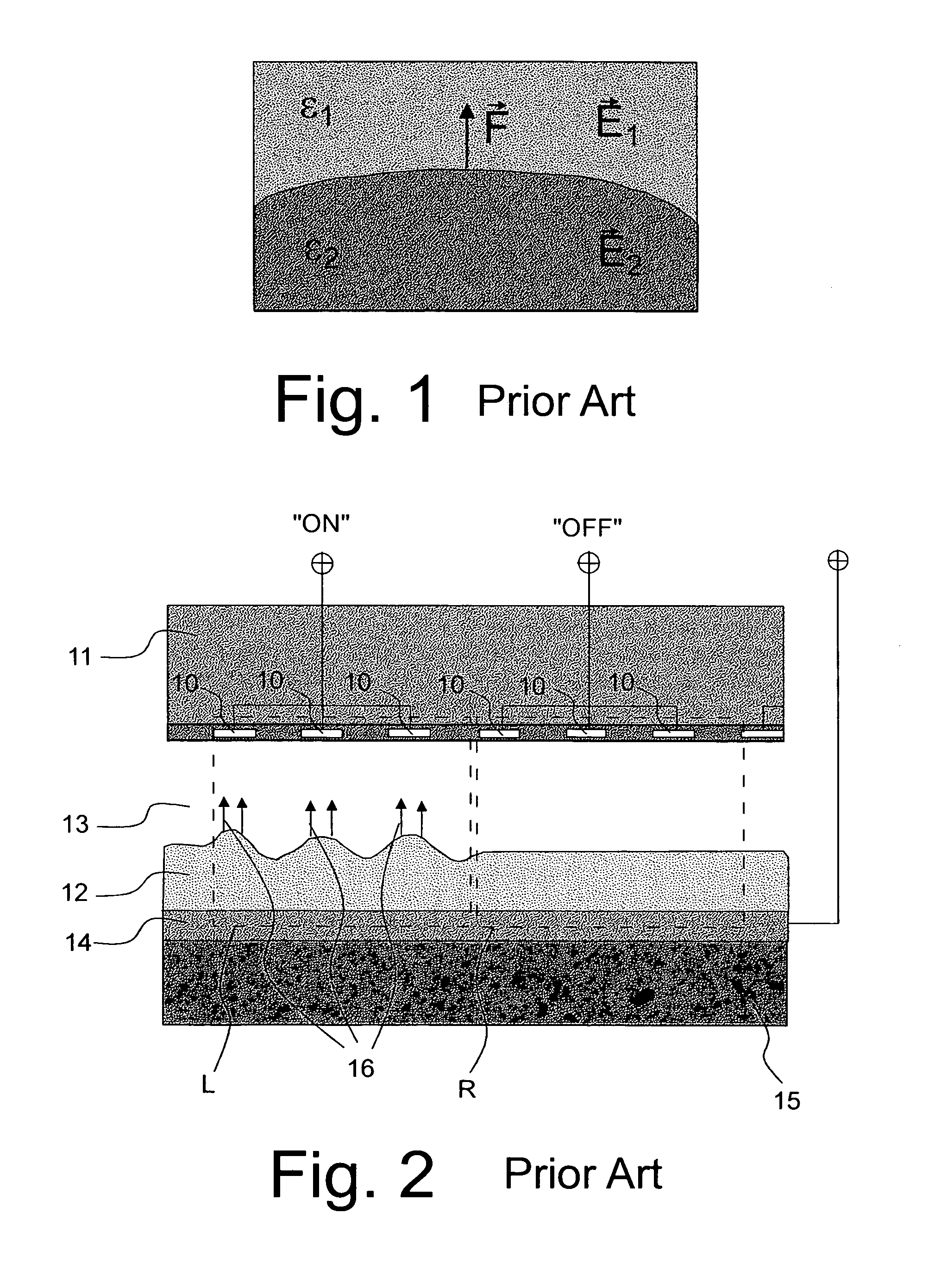
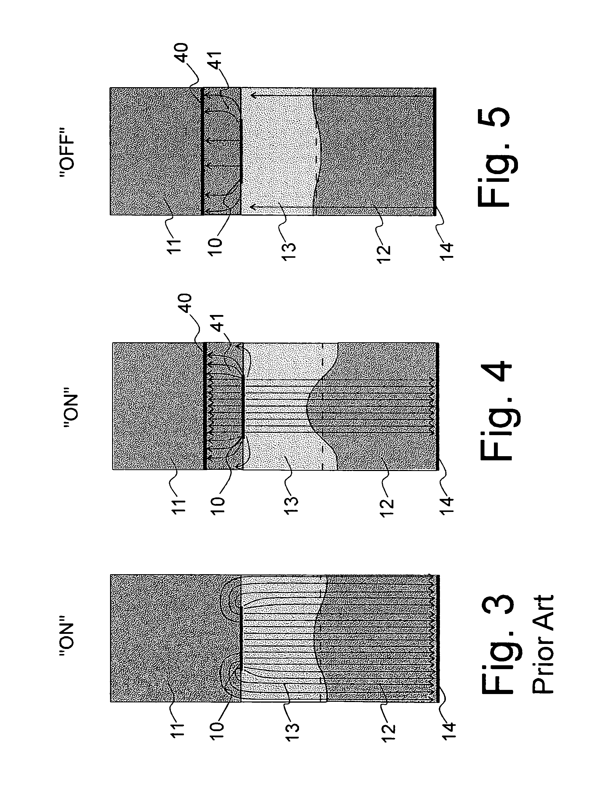
[0045]FIGS. 3-5 illustrate schematically a single sub-cell cell structure used for the numerical computer simulations. The sub-cell comprises one signal electrode 10 plus half the spacing to the next adjacent signal electrode on each side. Therefore, a complete cell comprises in this example case all together three adjacent signal electrodes in a manner similar than presented in FIG. 2. A practical cell (or pixel) can c...


PUM

PropertyMeasurementUnit
distanceaaaaaaaaaa
viscoelasticaaaaaaaaaa
electric fieldaaaaaaaaaa

Abstract

An electrically controlled light modulator device comprises at least one cell, where two deformable dielectric layers meet at an interface, at least one of said layers consisting of viscoelastic relief forming gel. A first support electrode structure and a second signal electrode structures are arranged on separate sides of the dielectric layers in order to create an electric field passing through said layers and in order to create surface reliefs on the viscoelastic gel layer. According to the invention, a third enhancement electrode structure is arranged in the proximity of the first signal electrode structure. Applying enhancement signal voltage between the enhancement electrode structure and the signal electrode structure concentrates locally the electric field passing through the two deformable dielectric layers and therefore enhances the amplitude of the deformation of the viscoelastic gel layer.

Description

CROSS-REFERENCE TO RELATED APPLICATION[0001]This application is the U.S. National Stage of International Application Number PCT / FI02 / 00512 filed 13 Jun. 2002 and published in English on 24 Dec. 2003 under International Publication Number WO 03 / 107087A1.FIELD OF THE INVENTION[0002]The present invention relates to electrically controlled light modulator devices. The present invention relates also to display devices comprising a plurality of said electrically controlled light modulator devices.BACKGROUND OF THE INVENTION[0003]Document WO 01 / 48531 discloses a display panel structure (see especially FIGS. 49 to 55) in the form of an array of cells each of which comprises two deformable dielectric layers, which meet at a common interface. One of said dielectrics can be air; the other is preferably polymer material acting as a relief forming gel. For each cell a first electrode structure, a support electrode structure is arranged on one side (below) of said dielectric layers and a second e...

Claims


Application Information

Patent Timeline
Patent Type & Authority Patents(United States)
IPC IPC(8): G02F1/07G02F1/03G02B26/02
CPCG02B26/004G02B26/02G03H2225/24G03H2225/32
Inventor SCHORPP, MARCUS
Owner NOKIA CORP
Why Eureka
Try Eureka