Integrated device with multiple reading and/or writing commands

a technology of integrated devices and commands, applied in the direction of memory allocation/allocation/relocation, program control, information storage, etc., can solve the problems of reduced access and transfer rate of communication interfaces, complex implementation of integrated devices in some specific applications, and inflexible known communication interfaces

Active Publication Date: 2008-05-20
STMICROELECTRONICS SRL
View PDF3 Cites 12 Cited by
  • Summary
  • Abstract
  • Description
  • Claims
  • Application Information

AI Technical Summary

Problems solved by technology

A drawback of such integrated devices is the fact that the communication interface reduces the access and transfer rate (because of the address and data multiplexing).
Furthermore, the known communication interfaces are not very flexible; this makes it rather complex to employ the integrated devices in some specific applications.
Further, the known integrated devices do not allow the exploitation at their best of the performance of the respective memories, for example, in applications requiring the repetition of consecutive reading or writing operations.

Method used


Image

  • Integrated device with multiple reading and/or writing commands
  • Integrated device with multiple reading and/or writing commands
  • Integrated device with multiple reading and/or writing commands

Examples


Embodiment Construction

[0019]Preferred embodiments of the present invention will be described in detail hereinbelow with reference to the attached drawings.

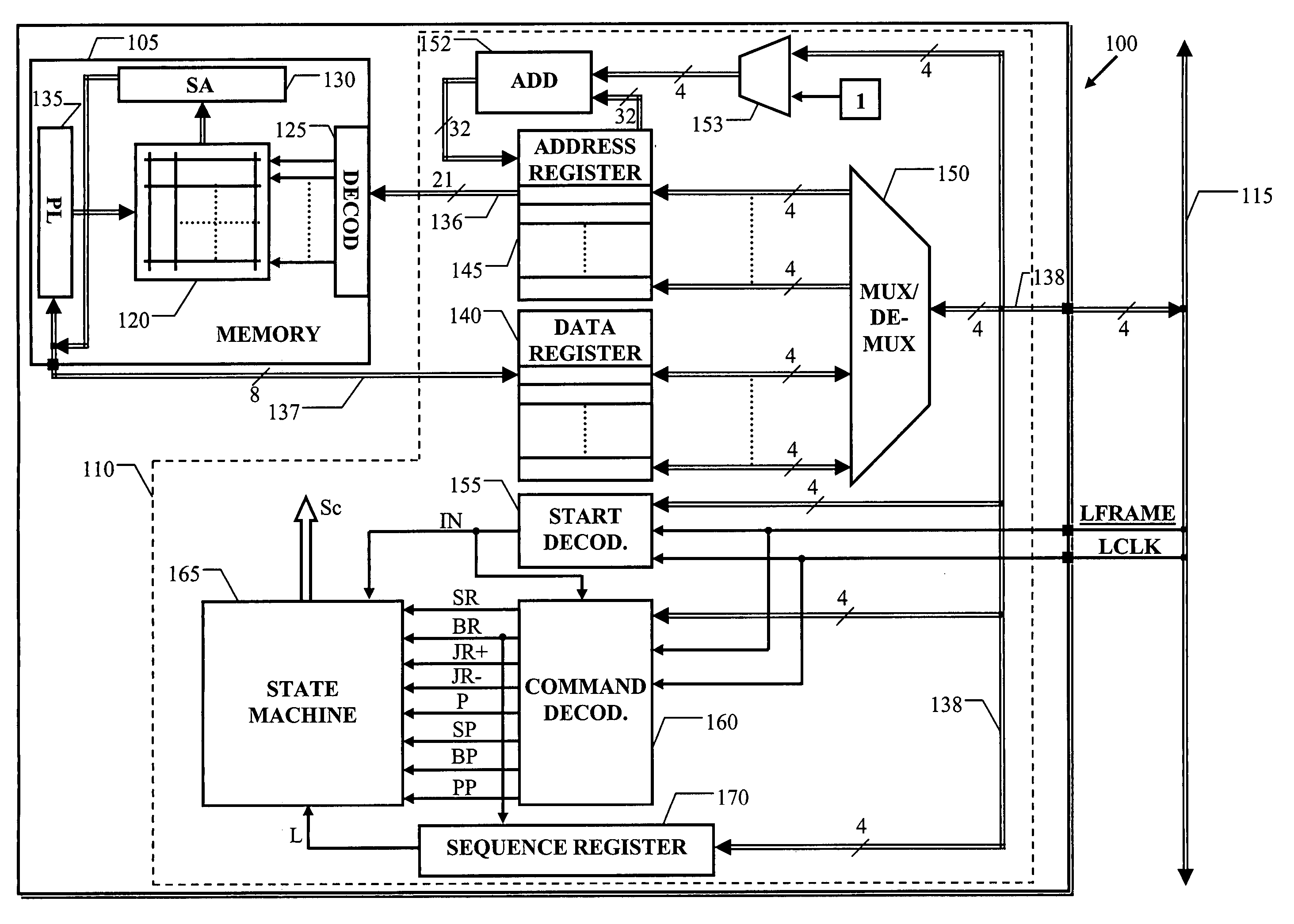
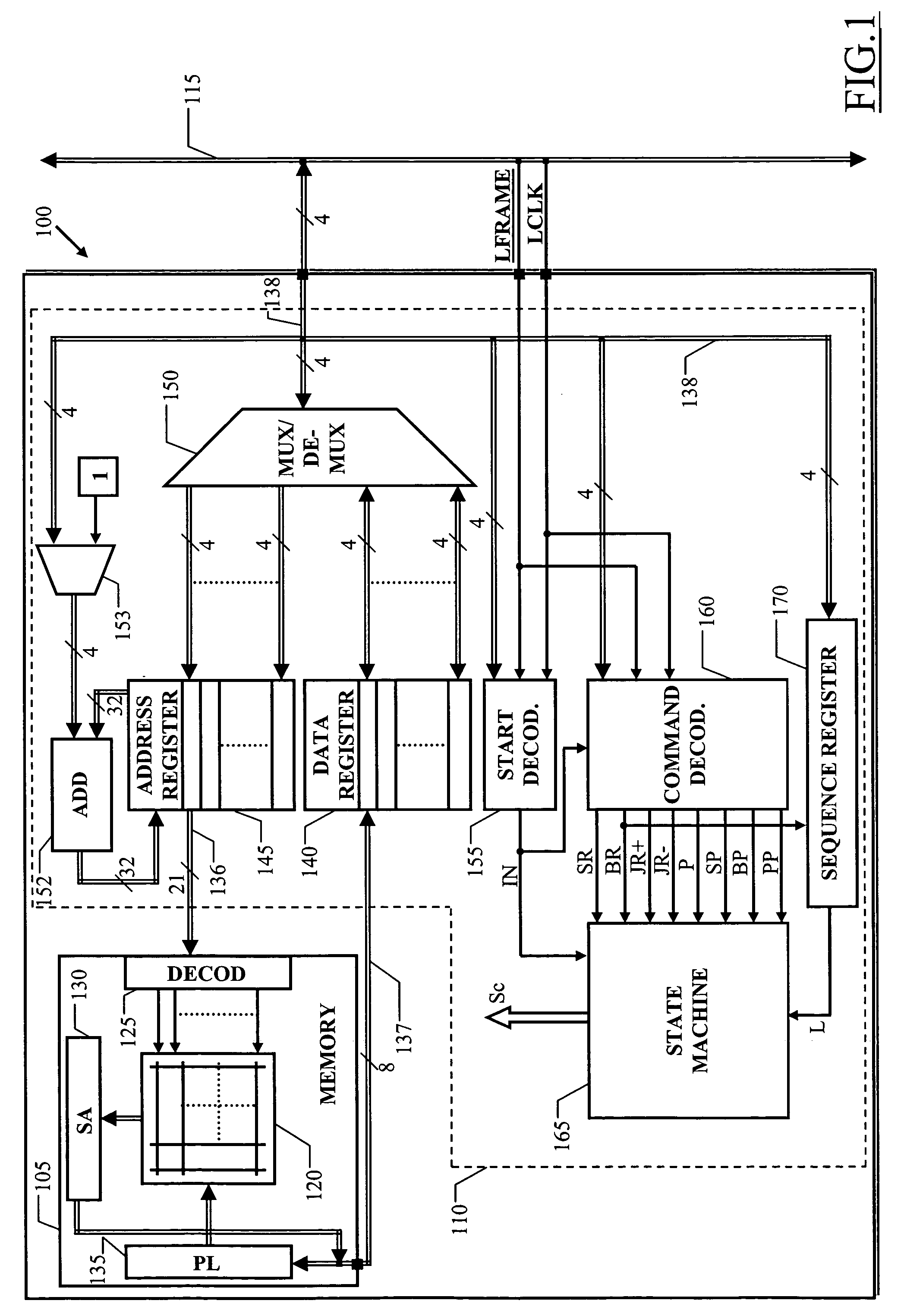
[0020]FIG. 1 shows a functional block diagram of an integrated device 100 according to an embodiment of the present invention. The integrated device 100 includes (in the same semiconductor chip) a semiconductor memory 105 and a communication interface 110 suitable to interface the memory 105 with external devices (not shown) through a suitable external communication bus 115. For example, such external devices can include a microprocessor, a microcontroller, a digital signal processor (DSP) and the like.

[0021]The memory 105 is a memory of the non-volatile type, such as an EEPROM memory of the Flash type. The memory 105 includes a matrix 120 of memory cells (for example, implemented by floating gate MOS transistors) that each store one bit. The memory 105 operates in parallel groups of bits, which define a word stored in a corresponding memory location. ...


PUM


Abstract

An integrated device is provided that includes a non-volatile memory having an addressing parallelism and a data parallelism, and a communication interface for interfacing the memory with an external bus. The external bus has a transfer parallelism lower than the addressing parallelism and the data parallelism. The communication interface includes control means for executing multiple reading operations and / or multiple writing operations on the memory according to different modalities in response to corresponding command codes received from the external bus. Also provided is a method of operating such an integrated device.

Description

CROSS-REFERENCE TO RELATED APPLICATIONS[0001]This application is based upon and claims priority from prior Italian Patent Application No. MI2003A001893, filed Oct. 3, 2003, the entire disclosure of which is herein incorporated by reference.FIELD OF THE INVENTION[0002]The present invention relates to an integrated memory device.BACKGROUND OF THE INVENTION[0003]In many applications it is important to employ integrated devices that are capable of interacting with other electronic apparatuses (for example, a microprocessor that needs to read the data stored in a non-volatile memory).[0004]Referring in particular to the field of memories, different communication protocols have been proposed with respective bus architectures for the communication. Particular attention has been addressed to protocols that allow operating with a low number of signals so as to limit the corresponding number of pins of the integrated device, and thus the cost and size thereof. An example of such protocols is ...

Claims


Application Information

Patent Timeline
Patent Type & Authority Patents(United States)
IPC IPC(8): G06F12/02G06F13/16G06F12/00G11C16/06
CPCG11C16/06G11C2216/30
Inventor POLIZZI, SALVATOREPERRONI, MAURIZIO FRANCESCOMAZZARA, SALVATORE
Owner STMICROELECTRONICS SRL
Why Eureka
Try Eureka