
Automated correction of asymmetric enclosure rule violations in a design layout

a technology of automatic correction and design layout, applied in computer aided design, program control, instruments, etc., can solve the problems of complex and time-consuming process of electronic circuit design, integrated circuit design, and high design effort for detailed design layou

Active Publication Date: 2008-05-27
ORACLE INT CORP
View PDF4 Cites 19 Cited by
  • Summary
  • Abstract
  • Description
  • Claims
  • Application Information

AI Technical Summary

Benefits of technology

"The patent describes a technique for automatically identifying and correcting design rule violations in electronic circuits. Specifically, it focuses on correcting asymmetric violations, such as endlap violations, which can occur when there is a metal layer and a via layer in the circuit design. The technique uses directional patches to expand the metal path only on the side of the via towards the end of the metal path. The patch is constructed based on the width, length, starting point, and direction of the violation. The technique can be implemented using a standalone EDA tool or through a command-line interface or a batch process. The technique also includes determining if the added patch causes other design rule violations and removing it if necessary. Overall, the technique improves the accuracy and efficiency of electronic circuit design."

Problems solved by technology

Design of an electronic circuit, for example, an integrated circuit (IC), is a complicated and time-consuming process. FIG. 1 illustrates a typical design flow of an integrated circuit device from conception through the generation of a fabrication ready design layout.
The detailed design layout may require a very intensive and time-consuming design effort and is typically performed utilizing specialized computer aided design (CAD) or Electronic Design Automation (EDA) tools.
DRC may be a time-consuming, iterative process that often requires manual manipulation and interaction by the designer.
Deep sub-micron designs typically have stringent design rules that are often not recognized or not properly handled by existing EDA tools, for example, automated place and route tools.
In such cases, if the metal nearest the end of the metal path does not overlap the via on that side by this greater amount, an endlap violation may occur.
However, it is difficult for conventional EDA tools to construct a design to meet these types of design rules, because most conventional EDA tools are two-dimensional programs that are good at treating objects in both dimensions simultaneously or symmetrically, but not asymmetrically.
Therefore, after routing, some metal paths created by conventional EDA tools, typically routing tools, may violate asymmetric endlap design rules.
However, unless carefully and often manually performed, patches may cause additional design rule violations.
For example, a metal patch placed over the end of a metal path may cause a minimum metal spacing rule violation or a jog rule violation.
Also, with existing tools, it may be difficult or impossible to determine the correct location, orientation and dimensions for such patches without time-consuming manual intervention by the designer.
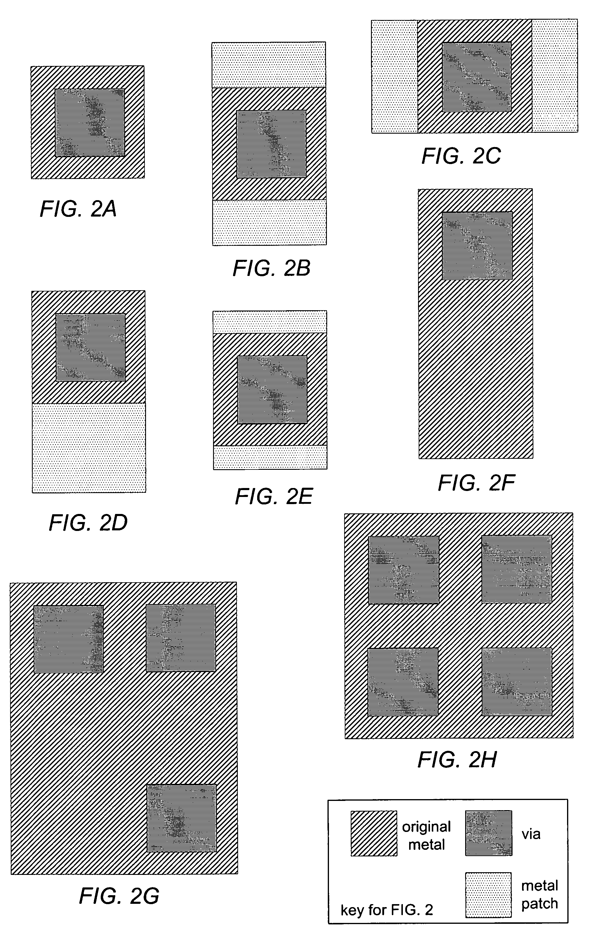
In another example involving both an endlap violation and a minimum area violation, a conventional EDA tool may not correct the minimum area violation by placing a patch centered on the via, due to the minimum spacing violation it may cause.
In this case, the geometries may still violate the endlap design rule.
In yet another example, a minimum area violation may be corrected by a conventional EDA tool placing a patch centered on the via, as shown in FIG. 2E, but the area difference between the patch and original metal geometry may be too small to correct an endlap design rule violation for the same geometries.
In these cases, a conventional EDA tool may not automatically correct the endlap violation.
In both of these cases, conventional EDA tools may not correct the endlap violations automatically.
Because routing tools may do much of their work as part of an automated flow, the number of endlap violations inadvertently generated may be huge.
In other cases, they may not be corrected by an existing automated flow.
Because EDA tools are increasingly relied upon to create design layouts, and because conventional EDA tools do not prevent the creation of certain violations, thousands of violations can be created that must be corrected.
Performing a DRC and manipulation of the design layout to correct these violations often requires manual interaction from the designer.
Creation of a violation-free design layout becomes a critical, time-consuming process.
Due to the complexity of the design and because the place and route design flow can be repeated throughout the design process, manually fixing violations may not be an affordable approach.

Method used


Image

  • Automated correction of asymmetric enclosure rule violations in a design layout
  • Automated correction of asymmetric enclosure rule violations in a design layout
  • Automated correction of asymmetric enclosure rule violations in a design layout

Examples


Embodiment Construction

[0036]One or more EDA tools may be used to place geometries on various layers of a design layout and to connect them together during creation of the design layout. During a Design Rule Check, or DRC, various design rules may be checked against the design layout. In a modern semiconductor design, it may be desirable to apply different sets of rules to the geometries (i.e., features) on a given layer depending upon their relative size. For example, many design layers, especially those that are used for implementing gates (e.g., polysilicon layers) and wires (e.g., metal layers) may be divided into different classes depending upon their minimum width in any dimension. Objects in different width classes, or ranges, may adhere to different design rules, such as spacing rules, via enclosure rules, and others, to improve wafer fabrication results.

[0037]An enclosure check is a common function that is available in most EDA tools performing a DRC. This type of check measures the enclosure of ...


PUM


Abstract

Automated techniques may correct certain rule violations, simplifying and automating the design layout of an electronic circuit, whether embodied as a design encoding or as a fabricated electronic circuit. Violations of enclosure design rules, those specifying the minimum amount that a geometry on a first layer must overlap a geometry on a second layer of a design layout, and more specifically, violations of asymmetric enclosure design rules, may be corrected using a geometric construction algorithm. This geometric construction algorithm may use the known width of the geometry on the second layer and a predetermined size factor to determine other parameters for constructing and placing a patch over a violation, such as the patch width, the patch length, the patch starting edge, and the patch direction. Patches may be constructed using different predetermined size factors when asymmetric enclosure violations are located on first layer geometries in different width ranges.

Description

BACKGROUND OF THE INVENTION[0001]1. Field of the Invention[0002]This invention relates to the layout of electronic circuits and more particularly to complex computer aided design layout and correction of rule violations in a design layout of, for example, an integrated circuit (IC) device or printed wiring board, in preparation for fabrication.[0003]2. Description of the Relevant Art[0004]Design of an electronic circuit, for example, an integrated circuit (IC), is a complicated and time-consuming process. FIG. 1 illustrates a typical design flow of an integrated circuit device from conception through the generation of a fabrication ready design layout. Generally, the design flow commences with defining the design specifications or requirements, such as required functionality and timing, as indicated at 110. The requirements of the design are implemented, for example, as a net-list or electronic circuit description, as indicated at 120. The implementation can be perfommed by, for exa...

Claims


Application Information

Patent Timeline
Patent Type & Authority Patents(United States)
IPC IPC(8): G06F17/50
CPCG06F17/5081G06F30/398
Inventor LI, MU-JING
Owner ORACLE INT CORP
Learn More