Chip resistor fabrication method
a technology of chip resistors and fabrication methods, which is applied in the direction of resistive material coating, semiconductor/solid-state device testing/measurement, instruments, etc., can solve the problems of difficult to cut the mother substrate properly and the substrate surface is difficult to be cut properly
- Summary
- Abstract
- Description
- Claims
- Application Information
AI Technical Summary
Benefits of technology
Problems solved by technology
Method used
Image

Examples
first embodiment
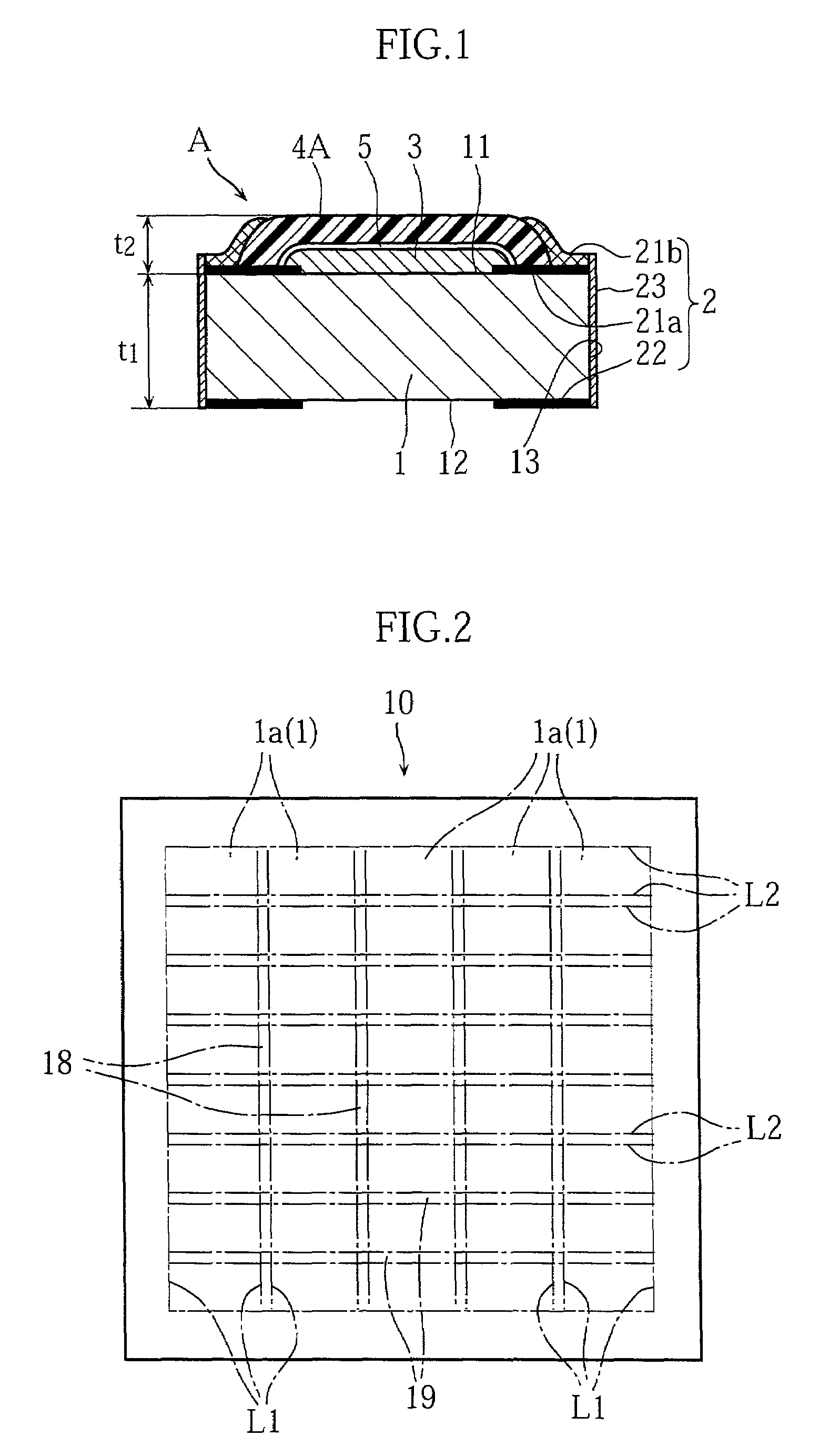
[0032]FIG. 1 shows the basic structure of a chip resistor (generally indicated by the reference A) according to the present invention. The resistor A, which is a surface-mounting type, includes a substrate 1 made of alumina ceramic. In the illustrated example, the thickness t1 of the substrate is about 0.18 mm. In plan view (not shown), the length of the substrate 1 is about 0.6 mm and the width is about 0.3 mm. The substrate 1 is provided with a pair of electrodes 2 each of which is disposed at an end of the substrate 1. A resistive layer 3 is formed on the upper surface of the substrate, bridging between the two electrodes 2.
[0033]As shown in FIG. 1, each electrode 2 is composed of a first upper conductive layer 21a (formed on the upper surface 11 of the substrate 1), a lower conductive layer 22 (formed on the lower surface 12 of the substrate 1), a second upper conductive layer 21b (formed on the first upper conductive layer 21a) and a side conductive layer 23 (formed on the side...
second embodiment
[0054]FIG. 11 shows the basic structure of a chip resistor according to the present invention. The resistor (generally indicated by the reference B) includes a two-layer substrate 1A, a pair of electrodes 2, a resistive layer 3, an overcoat 4 and an undercoat 5. Each of the electrodes 2 is composed of a first upper conductive layer 21a, a lower conductive layer 22, a second upper conductive layer 21b and a side conductive layer 23.
[0055]The substrate 1A is composed of a first layer 1Aa and a second layer 1Ab. These two layers are held in close contact with each other. The second layer 1Ab is made of a softer insulating material than the first layer 1Aa, so that it is more easily processed. Examples of such material are aluminum nitride, forsterite, etc. The Mohs hardness of these materials is about 7.0˜7.5, which is smaller than that of alumina ceramic (about 8.5˜9.0). The thickness t of the second layer 1Ab is about 20˜100 μm (preferably 25˜50 μm). The thickness of the substrate 1A...
third embodiment
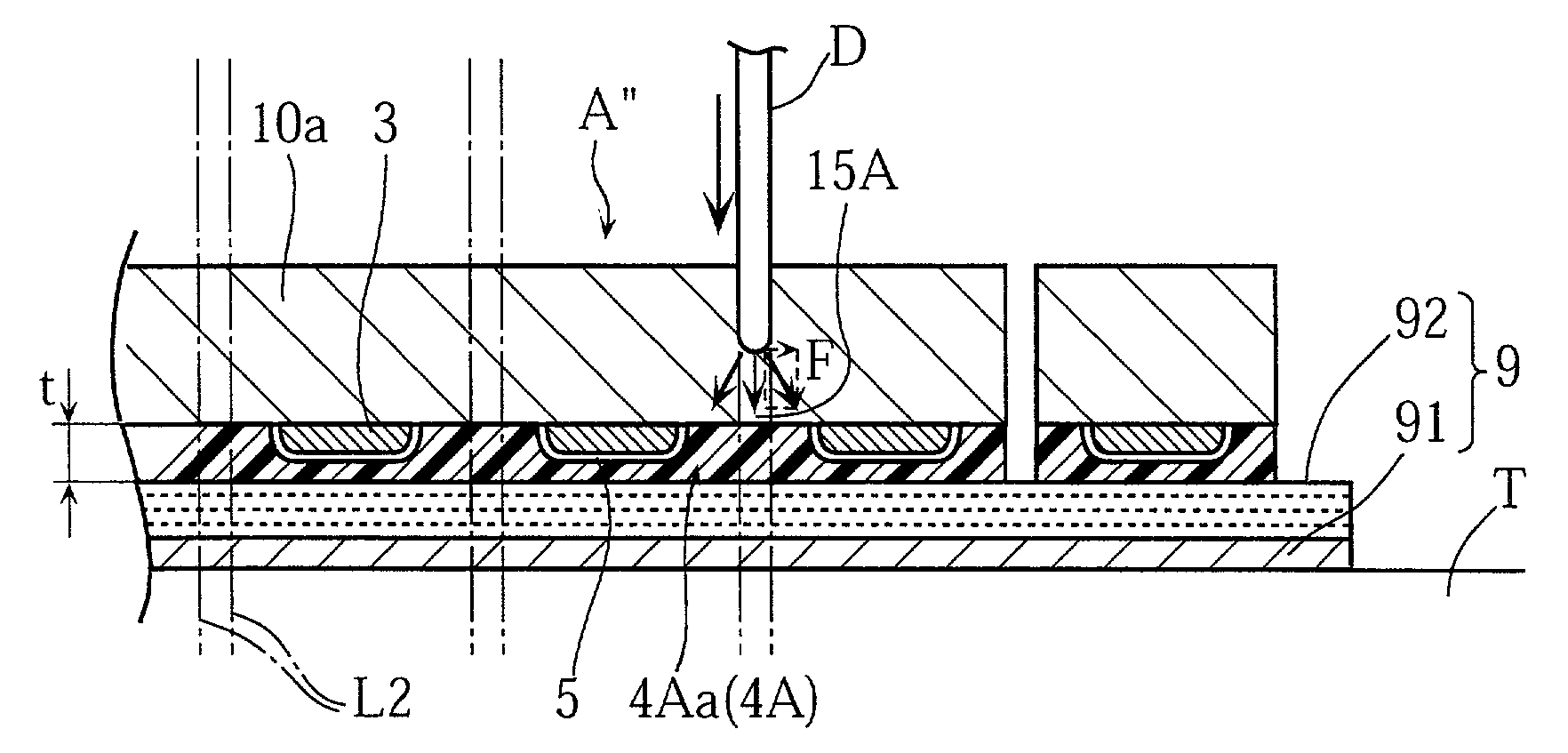
[0064]FIG. 15 shows the basic structure of a chip resistor according to the present invention. The resistor (generally indicated by the reference C) includes an alumina ceramic substrate 1, a pair of electrodes 2, a resistive layer 3, an overcoat 4 (made of glass) and an undercoat 5. Each of the electrodes 2 is composed of a first upper conductive layer 21a, a second upper conductive layer 21b, a lower conductive layer 22A and a side conductive layer 23.
[0065]The lower conductive layer 22A is made by printing and baking a conductive paste containing gold or silver. The thickness t of the layer 22A is about 20˜100 μm (preferably 25˜50 μm). The layer 22A is softer than the substrate 1, so that it can be readily processed.
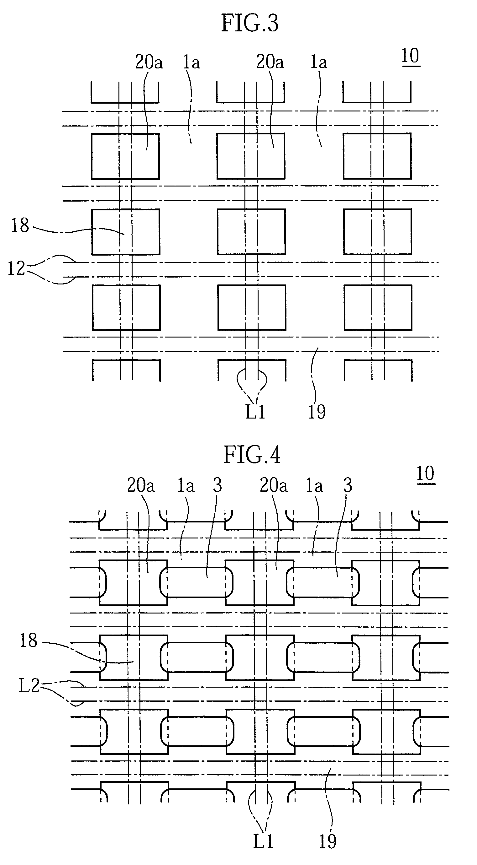
[0066]To fabricate the chip resistor C, first a mother substrate 10 (see FIG. 16) is prepared. Then, an upper conductive pattern (which is to provide the first upper conductive layer 21a) is formed on the upper surface of the substrate 10 by a screen printing techniqu...
PUM
| Property | Measurement | Unit |
|---|---|---|
| thickness | aaaaa | aaaaa |
| thickness | aaaaa | aaaaa |
| thickness t1 | aaaaa | aaaaa |
Abstract
Description
Claims
Application Information
 - R&D Engineer
- R&D Manager
- IP Professional
- Industry Leading Data Capabilities
- Powerful AI technology
- Patent DNA Extraction
Browse by: Latest US Patents, China's latest patents, Technical Efficacy Thesaurus, Application Domain, Technology Topic.
© 2024 PatSnap. All rights reserved.Legal|Privacy policy|Modern Slavery Act Transparency Statement|Sitemap