Level shift circuit and method for the same

a level shift circuit and level shift technology, applied in logic circuits, pulse automatic control, pulse technique, etc., can solve the problem of even longer time delay, and achieve the effect of speeding up output voltage level switching

Active Publication Date: 2008-06-03
RICHTEK TECH
View PDF3 Cites 11 Cited by
  • Summary
  • Abstract
  • Description
  • Claims
  • Application Information

AI Technical Summary

Benefits of technology

[0009]A first objective of the present invention is to provide a level shift circuit which provides current to its output terminal from the source of the second operational voltage to speed up the output voltage level switching.
[0011]A third objective of the present invention is to provide a method to achieve faster output voltage level switching with reduced power consumption.
[0012]To achieve the foregoing objectives, according to an aspect of the present invention, a level shift circuit comprises: level shift means for converting an input of a first operational voltage to an output of a second operational voltage, and a current path connecting with a source of the second operational voltage and providing current to an output terminal of the level shift means for speeding up output voltage level switching.

Problems solved by technology

The time delay is even longer if the level gap between the first and the second operational voltages is considerably large, which is of course undesirable.

Method used


Image

  • Level shift circuit and method for the same
  • Level shift circuit and method for the same
  • Level shift circuit and method for the same

Examples


Embodiment Construction

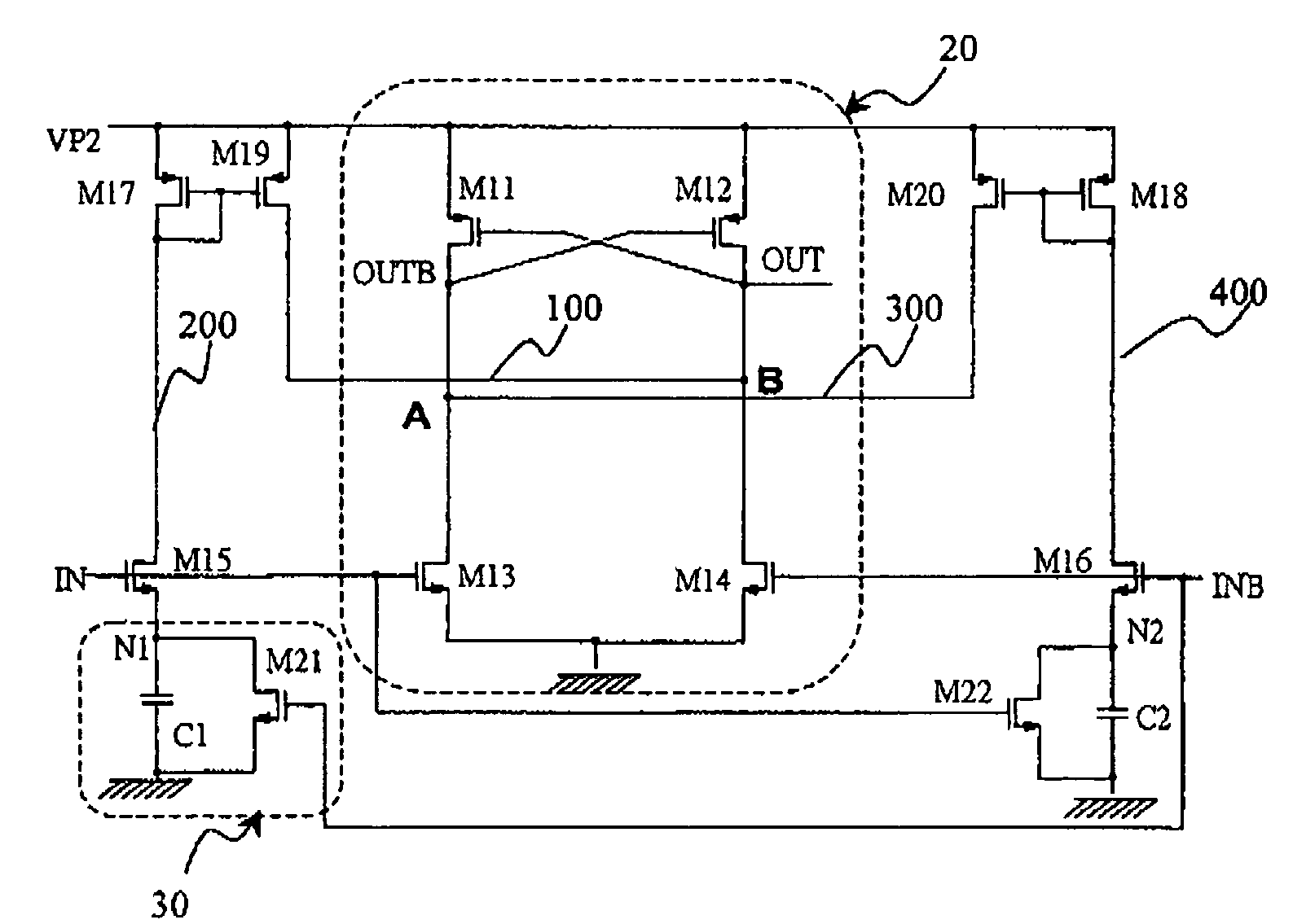
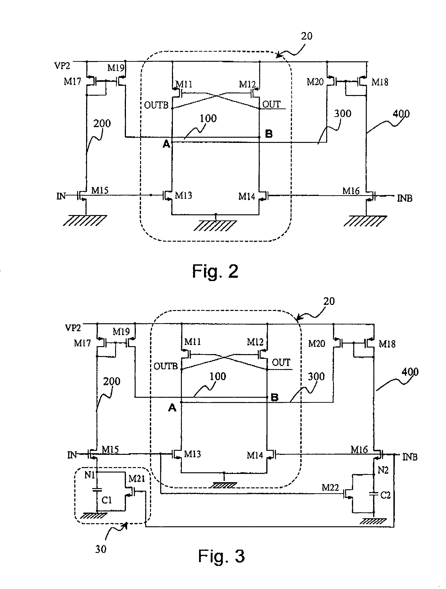
[0029]For purpose of simplicity, in all of the following embodiments, it is assumed that the first operational voltage is 5V and the second operational voltage VP2 is 23V. However, the present invention should not be limited to such arrangement, but may be applied to level shift between any two voltage levels.

[0030]FIG. 2 schematically shows a first preferred embodiment according to the present invention. As shown in the figure, a level shift circuit comprises a pair of PMOS transistors M11 and M12, and a pair of NMOS transistors M13 and M14 (the PMOS and NMOS pairs constituting basic level shift means 20). In addition to the above, the level shift circuit according to this embodiment further comprises a current path 100 (VP2-M19-node B) which is connected to the source for supplying the second operational voltage VP2. The current path serves to pull high the voltage level at the node B, as explained below.

[0031]More specifically, referring to FIG. 2, when the input IN switches from...


PUM


Abstract

The present invention discloses a level shift circuit which comprises: level shift means for receiving an input of a first operational voltage and generating an output of a second operational voltage; and a current path connecting with a source of the second operational voltage and providing current to the output of the level shift means to speed up output level switching. The circuit preferably further comprises a power consumption control circuit for stopping excess power consumption when the output of the level shift means has substantially accomplished level switching.

Description

BACKGROUND OF THE INVENTION[0001]1. Field of the Invention[0002]The present invention relates to a level shift circuit, and in particular to a level shift circuit with faster output level switching, and a method for the same.[0003]2. Description of the Related Art[0004]A level shift circuit is for use to convert a DC voltage level from low to high (such as from 5V to 12V or 23V, etc.), or from high to low (such as from 12V to 5V or 3V, etc.); a level shift circuit is often used in a power control circuit chip. FIG. 1A shows the basic structure of a conventional level shift circuit 10, which comprises two PMOS transistors M1 and M2, and two NMOS transistors M3 and M4. Assuming the function of the circuit is to convert the voltage level from 5V to 23V, the input IN in the shown circuit may thus be an operational voltage of 5V (the first operational voltage), and the voltage supplied from the voltage source VP2 may be 23V (the second operational voltage).[0005]Referring to FIGS. 1A and...

Claims


Application Information

Patent Timeline
Patent Type & Authority Patents(United States)
IPC IPC(8): H03L5/00
CPCH03K3/012H03K3/35613
Inventor LIN, PAO-CHUANSU, HUNG-DERCHEN, AN-TUNGLIU, JING-MENG
Owner RICHTEK TECH
Why Eureka
Try Eureka