Contact image sensor and methods for aligning a light element array substrate thereof

a technology of contact image sensor and array substrate, which is applied in the direction of discharge tube/lamp details, instruments, radiation control devices, etc., can solve the problems of reducing image quality, difficult to integrally form such a light-shielding film, and unnecessary light entering the adjacent area, etc., to achieve convenient power supply to the light source, the effect of easy online alignmen

Inactive Publication Date: 2008-06-10
NIPPON SHEET GLASS CO LTD
View PDF3 Cites 31 Cited by
  • Summary
  • Abstract
  • Description
  • Claims
  • Application Information

AI Technical Summary

Benefits of technology

[0013]The object of the present invention is to solve the above-described problems. In accordance with the present invention, a method for aligning a light-receiving element array substrate in a short time, a method for manufacturing a contact image sensor, and a contact image sensor comprising components which have a suitable structure to facilitate the alignment of the light-receiving element array substrate are provided. The components include a plurality of micro-lens array plates, a slit plate and at least one light-receiving element array mounted on the substrate.
[0014]A first aspect of the present invention is a method for aligning a light-receiving element array substrate provided in a contact image sensor. In accordance with this method, the light-receiving element array substrate is aligned in a sub-scanning direction so that sensor-output detected through at least one light-receiving element array becomes a maximum while light reflected from a reference original of uniform lightness distribution is received by the at least one light-receiving element array mounted on the light-receiving element array substrate, the sub-scanning direction being perpendicular to the main-scanning direction. The reference original used to align the light-receiving element array substrate in accordance with the present invention has uniform lightness distribution. An original of high reflectivity with which sensor-output becomes large is preferably used for such a reference original to facilitate aligning the light-receiving element array substrate. A reference original with uniform lightness distribution may be an original with a chromatic color or an achromatic color (white or gray).
[0015]In addition, a second aspect of the present invention is another method for aligning a light-receiving element array substrate provided in a contact image sensor. In accordance with this method, the light-receiving element array substrate is aligned in a sub-scanning direction, so as to incline an array-line of at least one light-receiving element array with respect to a centerline of a slit opening to reduce the difference of distribution in a main-scanning direction of sensor-output while light reflected from a reference original of uniform lightness distribution is received by the at least one light-receiving element array mounted on the light-receiving element array substrate.
[0019]Moreover, a gap (allowance) is provided between the light-receiving element array substrate and the housing to enable the alignment of the substrate. Because the light-receiving element array substrate is supported in the housing while keeping the gap in which each of the light source, the slit plate and the lens other than the substrate is, fixed into the housing, the substrate may be aligned while monitoring the electric signal. Thus, a method is provided for aligning a light-receiving element array substrate in a short time, because only the substrate may be aligned.
[0020]Particularly, in accordance with the present invention, it becomes easy to implement the online alignment because the shape of the light-receiving element array substrate is formed so as to facilitate the application of power to the light source.
[0021]More particularly, in accordance with the present invention, there is provided a contact image sensor having a large sensor-output that corresponds to large amount of light without substantially increasing electrical current of the light-emitting element array, because an irregular amount of light caused by the light source and / or the lens may be suppressed.

Problems solved by technology

Although the light reflected from the original enters the lens and the light-receiving element in the contact image sensor receives the focused light by the lens, ghost images may be generated by the structure of an optical system causing a decrease in an image quality.
In addition, the rod lens array is generally formed by containing a light-shielding film between the rod lenses to obtain a more high-quality image, so that unnecessary light may not be entered into the adjacent rod lens.
On the micro-lens array plate, it is difficult to integrally form such a light-shielding film between micro-lenses, because the micro-lens array plate is formed integrally in the manufacturing process by means of injection molding of resin.
Therefore, ghost images become a significant matter when utilizing the micro-lens array plate for the lens of a contact image sensor as opposed to utilizing the rod lens array for the lens of the contact image sensor where ghost images are not typically generated.
Even if the slit plate is used, however, ghost images may be generated when precise alignment among the slit plate, the lens and the light-receiving element array is not carried out.
However, when the test chart 12 shown in FIG. 1A is used, there is a problem of taking more time for the alignment because the whole area of the test chart 12 should be read, and of a difficulty of online alignment.
In addition, in the case of utilizing the micro-lens array plate for the optical system, there is another problem in that the micro-lens array plate, especially, increases the irregular distribution of amount of light corresponding to the sensor-output relative to the case of utilizing another lens (e.g. a rod lens array).
It is typically difficult to form the micro-lens array plate while keeping a uniformity of the dimensions (in particular, the plate thickness) and an optical performance of micro-lenses (a direction of an optical axis, a lens pitch and a curvature of the lens) on the whole area of the micro-lens array plate in the injection molding process.

Method used


Image

  • Contact image sensor and methods for aligning a light element array substrate thereof
  • Contact image sensor and methods for aligning a light element array substrate thereof
  • Contact image sensor and methods for aligning a light element array substrate thereof

Examples


first embodiment

A First Embodiment

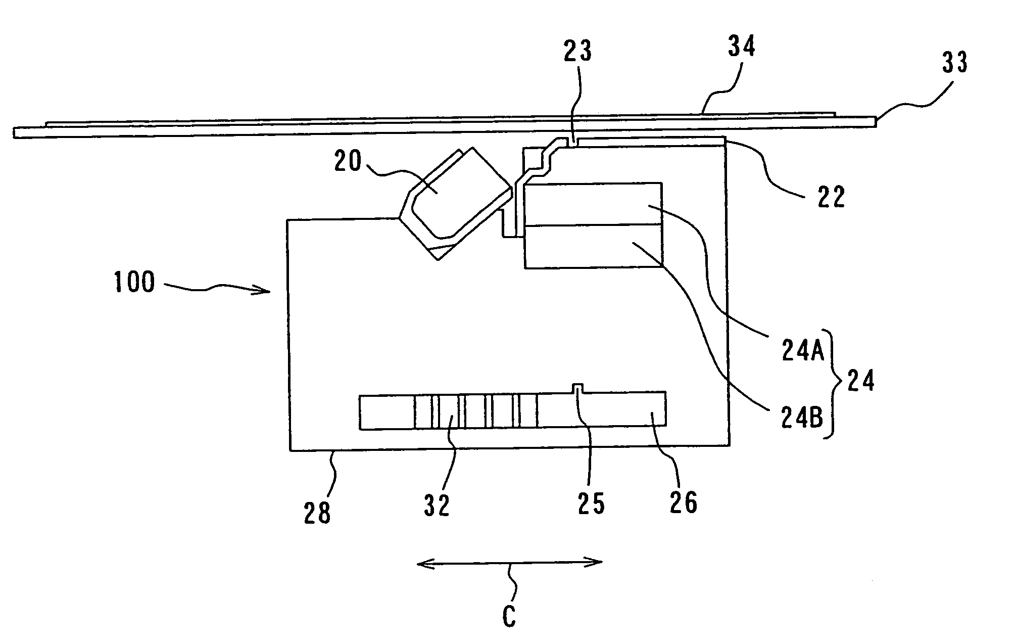
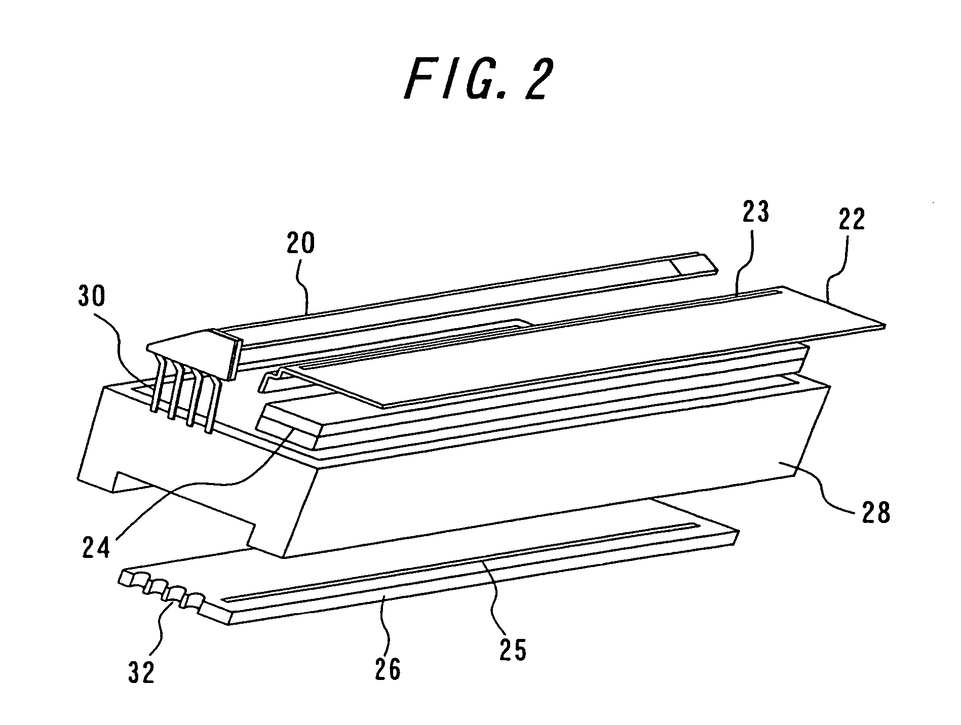
[0045]FIG. 2 is an exploded perspective view of a contact image sensor in accordance with the present invention. This contact image sensor comprises a light source 20, a slit plate 22, an erecting unit magnification lens 24 including stacked two micro-lens array plates 24a and 24b (FIG. 3), a light-receiving element array substrate 26 on which a light-receiving array 25 is mounted and a housing 28 for containing these components.

[0046]The light source 20 is composed of a linear illuminating device, such as one type of device in which the light-emitting element array is linearly located in a main-scanning direction and another type of device in which one or more of the light-emitting elements is located on one or both ends of a linear light-guide in the line illuminating device.

[0047]In this embodiment, an exemplary light source may include one or more of light-emitting elements. In an exemplary embodiment, the light source contains three light-emitting diodes (LEDs...

second embodiment

A Second Embodiment

[0068]A second embodiment, includes a method for aligning a light-receiving element array substrate 26 provided in a contact image sensor. The method may be implemented by the same structure as the contact image sensor shown in the above-described FIG. 7, thus a description of the structure is omitted with regard to similar components or elements. Normally, light irradiated by means of a light source generates an irregular distribution of the amount of light in a main-scanning direction. Therefore, the method includes the step of receiving light reflected from a reference original of uniform lightness distribution (for example, a white color original) by means of the light source to detect sensor-output through a light-receiving element array. The method further includes the step of aligning the light-receiving array substrate 26 in the sub-scanning direction such that an array-line of a light-receiving array 25 mounted on the substrate 26 is inclined with respect...


PUM


Abstract

A contact image sensor is provided including a housing, a slit plate a lens, one or two light sources and a light-receiving element array mounted on a light-receiving element array substrate. The housing contains the slit plate, the lens, the one or two light sources and the light-receiving element array substrate. The optical system of the contact image sensor is aligned and one or more depressions are formed on an end of the substrate for the alignment. Power to the one or two light sources is applied through one or more leads. Each of the one or more depressions is large enough so that each of the leads can be passed through the respective depressions.

Description

BACKGROUND OF THE INVENTION[0001]1. Field of the Invention[0002]The present invention relates to a method for aligning a light-receiving element array substrate provided in a contact image sensor in a sub-scanning direction, a method for manufacturing the contact image sensor, and the contact image sensor.[0003]2. Related Background Art[0004]A contact image sensor, which enables reading the image of an original, comprises a light source, a lens, a light-receiving element array (e.g. CCD) and a housing for containing them. The original is irradiated by light from the light source, the lens focuses the light reflected from the original on the light-receiving element array, and the light-receiving element array receives the focused light. Although the light reflected from the original enters the lens and the light-receiving element in the contact image sensor receives the focused light by the lens, ghost images may be generated by the structure of an optical system causing a decrease i...

Claims


Application Information

Patent Timeline
Patent Type & Authority Patents(United States)
IPC IPC(8): H01L27/00
CPCH04N1/0318H04N2201/02412H04N2201/02429H04N2201/02441H04N2201/02456H04N2201/0247H04N2201/02483H04N2201/03112H04N2201/03141H04N2201/03145H01L27/146
Inventor SAITOU, TOMIHISAYOSHIDA, HARUNOBUWAKISAKA, MASAHIDEKITAOKA, MASAKI
Owner NIPPON SHEET GLASS CO LTD
Why Eureka
Try Eureka