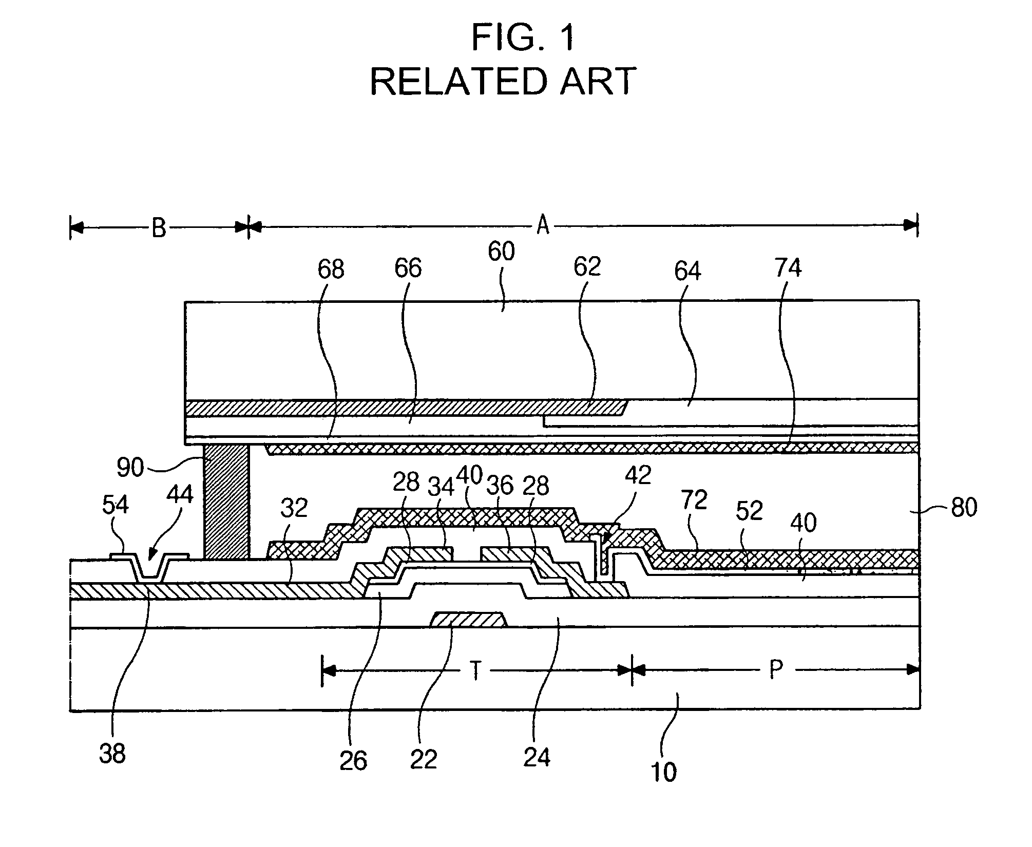
Array substrate for liquid crystal display device and method of manufacturing the same
- Summary
- Abstract
- Description
- Claims
- Application Information
AI Technical Summary
Benefits of technology
Problems solved by technology
Method used
Image

Examples
Embodiment Construction
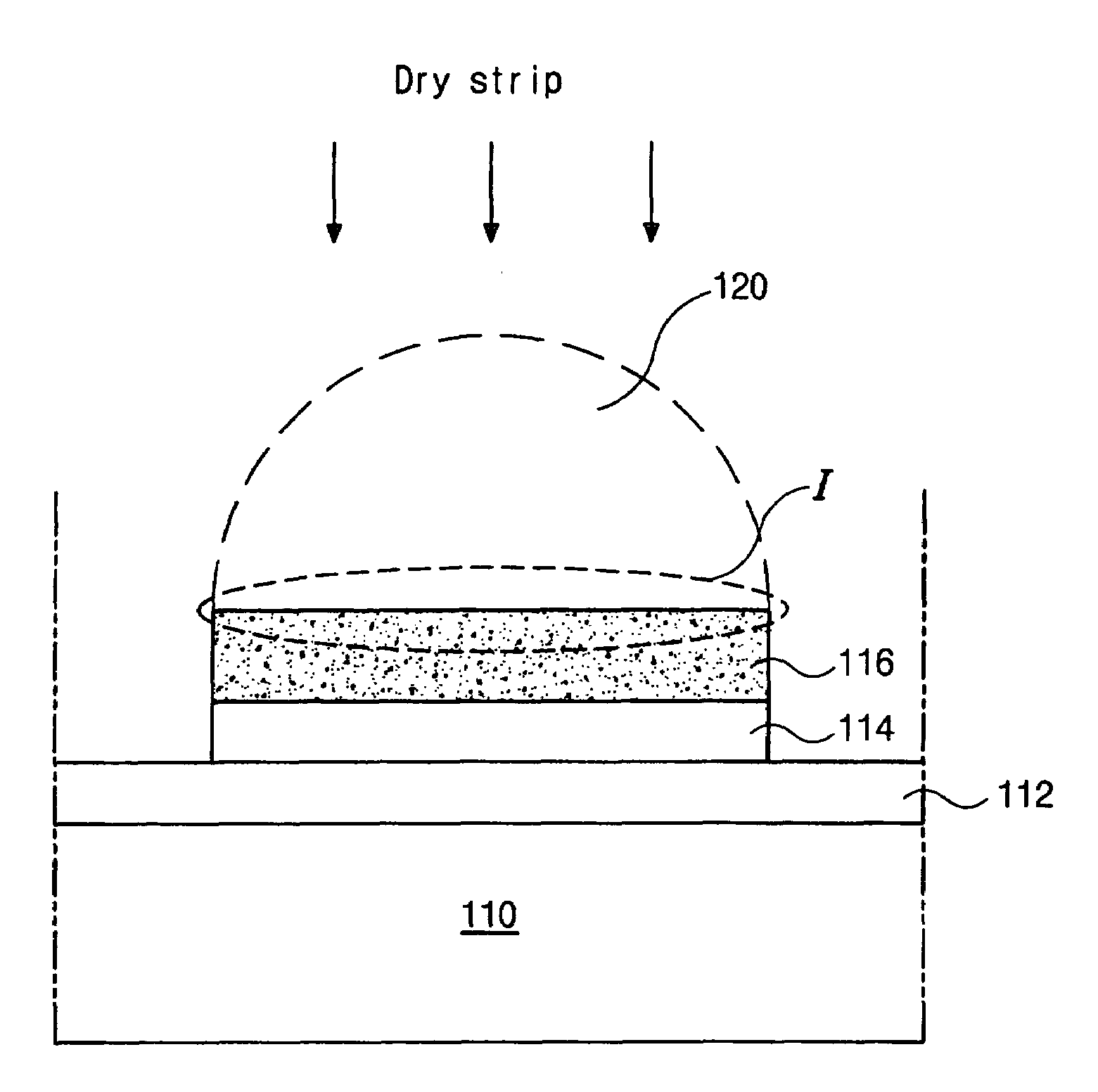
[0029]Reference will now be made in detail to the illustrated embodiments of the present invention, example of which is illustrated in the accompanying drawings.
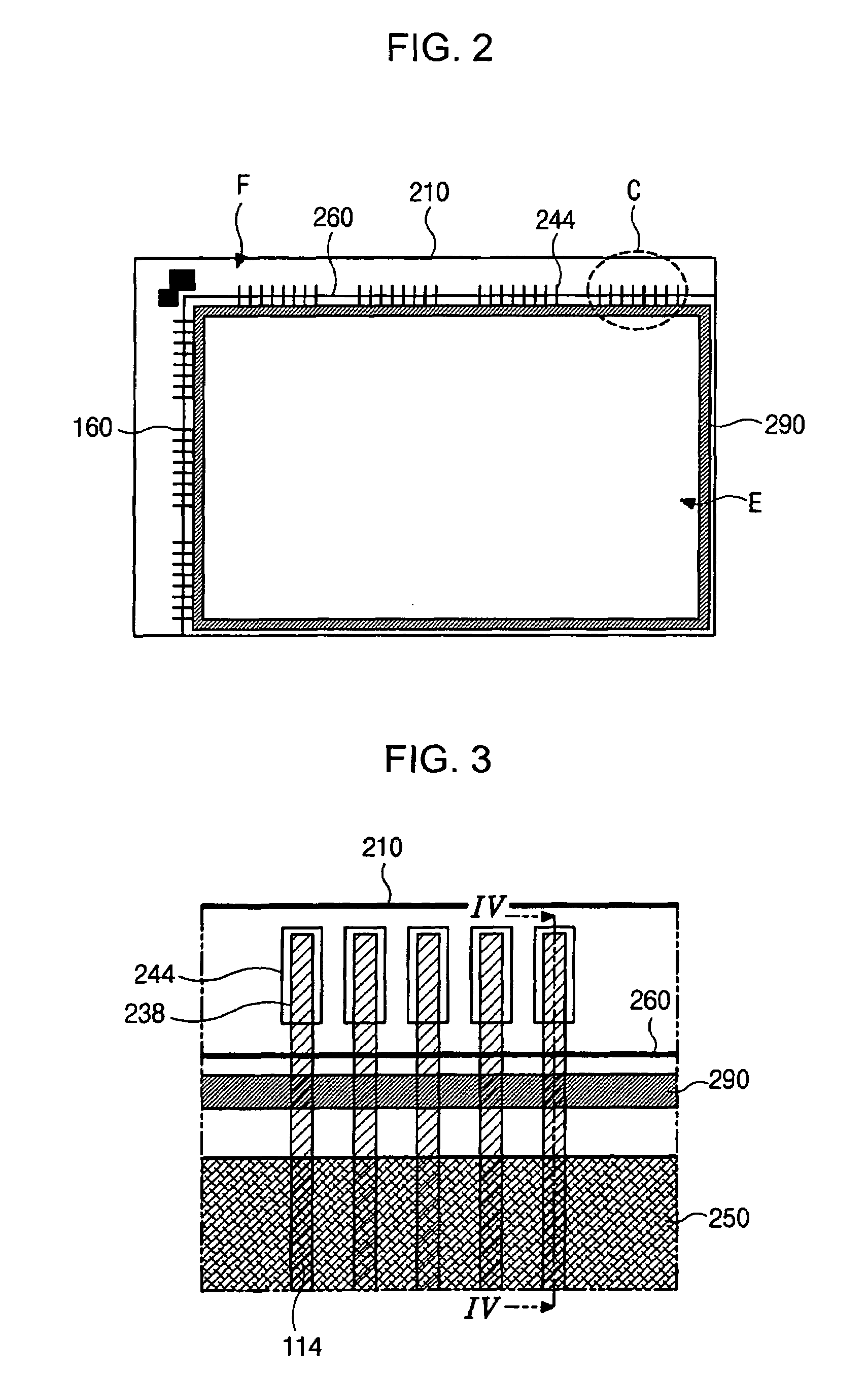
[0030]FIG. 2 is a plan view of an exemplary liquid crystal display (LCD) device according to the present invention. First and second substrates 210 and 260 are overlapped with a seal pattern 290 interposed between the two substrates 210 and 260. The first substrate 210 is wider than the second substrate 260. The LCD device can be divided as a display region E and a non-display region F. The display region E is surrounded by the seal pattern 290, and the non-display region F has pad portions 160 and 170.
[0031]FIG. 3 is an enlarged view of a portion C of FIG. 2 and FIG. 4 is a cross sectional view taken along line IV-IV of FIG. 3. On the substrate 210 there is formed a gate electrode 222 by depositing a first metal layer, and patterning the first metal layer through a first mask process. The gate electrode 222 may extend from ...
PUM
 Abstract
Description
Claims
Application Information
 - R&D Engineer
- R&D Manager
- IP Professional
- Industry Leading Data Capabilities
- Powerful AI technology
- Patent DNA Extraction
Browse by: Latest US Patents, China's latest patents, Technical Efficacy Thesaurus, Application Domain, Technology Topic.
© 2024 PatSnap. All rights reserved.Legal|Privacy policy|Modern Slavery Act Transparency Statement|Sitemap