Image sensing module and process for packaging the same

a technology of image sensing and processing equipment, applied in the field of image sensing modules, can solve the problems of large error, large transporting error, and customization that contradicts to the demanding requests, and achieves the effects of reducing transporting and tilting errors, reducing errors, and precise positioning

Inactive Publication Date: 2008-06-17
TONG HSING ELECTRONICS IND LTD
View PDF5 Cites 7 Cited by
  • Summary
  • Abstract
  • Description
  • Claims
  • Application Information

AI Technical Summary

Benefits of technology

[0008]A main object of the present invention is to provide a process for packaging an image sensing module, which utilizes a plurality of holes and positioning posts to achieve precise positioning required by the image sensing module. Thus, smaller modules, lower transporting and tilting errors, higher yields, better aligning precisions, lower costs, and a modulized design and a process without any precise positioning equipment can be obtained.

Problems solved by technology

Due to the mechanical limitations of those portable mobile devices, when the image sensing modules are applied to the portable mobile devices, custom-made modules are required to fit in the limitations.
However, customization contradicts to the demanding requests, such as low cost, quick development and mass production.
However, some drawbacks accompany both processes.
Further, surface mounting technology (referred to SMT hereinafter) and a printed circuit board (referred to PCB hereinafter) are utilized to conduct positioning between the lens and the image sensor, and therefore the error is relatively large.
Furthermore, in this process, a larger transporting error occurs since the shape of the glass or the substrate is generally square and thus larger clearance between the lens and the edges of the glass / substrate is required.
Additionally, since the lens holder is directly mounted on the glass, the tilting error of the whole image sensing module increases due to the error between the lens and the glass.

Method used


Image

  • Image sensing module and process for packaging the same
  • Image sensing module and process for packaging the same
  • Image sensing module and process for packaging the same

Examples


Embodiment Construction

[0030]The features and advantages of the present invention will become better understood with regard to the following embodiments. It is understood to those skilled in the art that the present disclosure of embodiments will be made by means of examples only and that numerous changes in the arrangement and combination of parts may be resorted without departing from the spirit and scope of the invention as claimed.

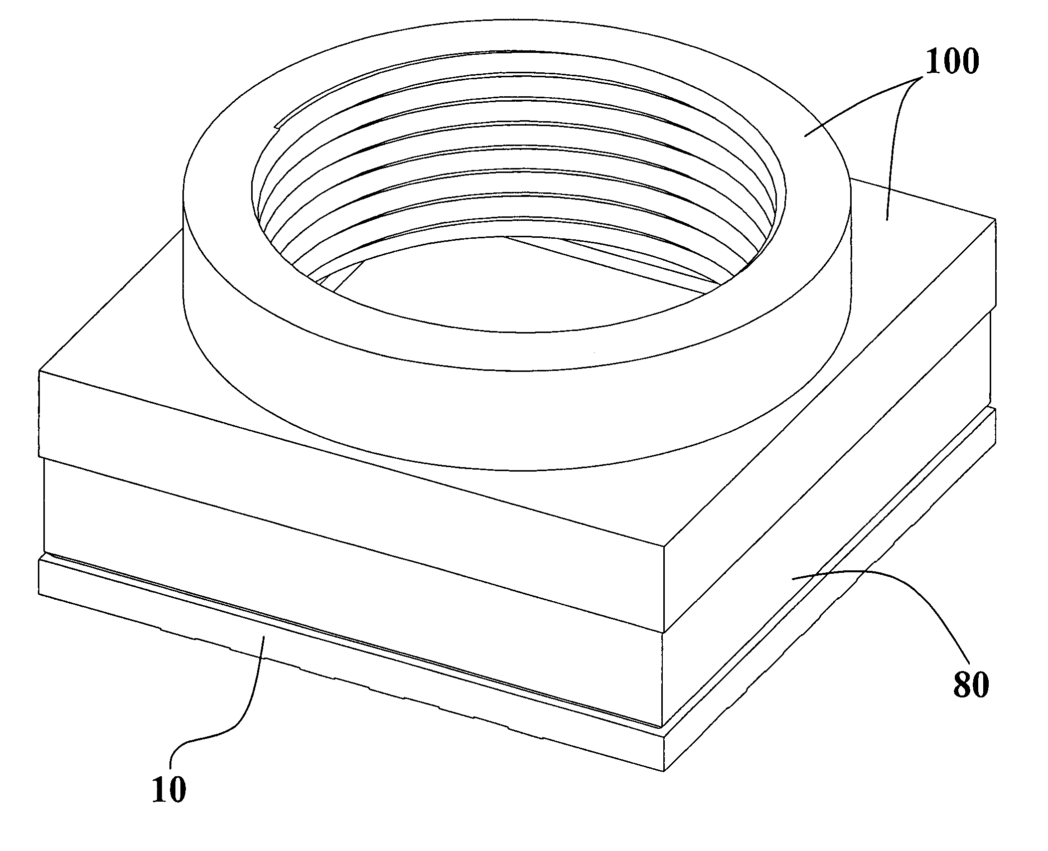
[0031]FIG. 5 is a schematic view showing an image sensing module according to an embodiment of the present invention. As shown in FIG. 5, the image sensing module 1 comprises a substrate 10, a plurality of electrically conductive pads 20, a plurality of component mounting areas 30, a plurality of surface mounting components 40, an image sensing component 60, a cover 80, a window 90, and a lens holder 100.

[0032]The substrate 10 is made of a ceramic or organic material, and the electrically conductive pad 20, and the component mounting areas 30 can be fabricated on the substra...


PUM


Abstract

An image sensing module includes: a substrate provided with at least two holes at corners and along edges thereof, a plurality of electrically conductive pads arranged in parallel along the edges of the substrate, a plurality of component mounting areas arranged in parallel on the substrate, a plurality of surface mounting components, each of which is mounted on each of the plurality of component mounting areas, an image sensing component mounted on the substrate and surrounded by the plurality of electrically conductive pads and the plurality of the component mounting areas, a cover provided with at least two positioning posts on one face thereof in correspondence with the holes to form a cavity enclosing the plurality of the electrically conductive pads and the plurality of the component mounting areas, the cover being further provided with at least two holes at corners and along edges on the other face thereof, a window fixed on the cover for isolating the module from its surroundings and allowing light to transmit there through, and a lens holder provided with at least two positioning posts for connecting with the holes of the cover.

Description

FIELD OF THE INVENTION[0001]The present invention generally relates to an image sensing module and a process for packaging such an image sensing module, and more particularly relates to an image sensing module applicable for a portable mobile device and a process for packaging the same.BACKGROUND OF THE INVENTION[0002]Image sensing modules are commonly applied to portable mobile devices such as digital still cameras, cellular phones and PDAs (Personal Digital Assistants). Due to the mechanical limitations of those portable mobile devices, when the image sensing modules are applied to the portable mobile devices, custom-made modules are required to fit in the limitations. However, customization contradicts to the demanding requests, such as low cost, quick development and mass production.[0003]Conventionally, an image sensing module is packaged by the following steps: forming a substrate having a cavity with a ceramic or organic material, gluing an image sensing component on the subs...

Claims


Application Information

Patent Timeline
Patent Type & Authority Patents(United States)
IPC IPC(8): H01J5/02G03B17/02H01J40/14H01L23/02H04N5/225
CPCH01L27/14618H01L27/14625H01L31/0203H01L2224/48091H01L2224/48227H01L2924/00014H01L2924/19105
Inventor CHANG, CHIA-SHUAIWU, CHIA-MING
Owner TONG HSING ELECTRONICS IND LTD
Why Eureka
Try Eureka