
Trench power MOSFET fabrication using inside/outside spacers

a technology of inside/outside spacers and mosfets, which is applied in the direction of basic electric elements, electrical equipment, semiconductor devices, etc., can solve the problems of difficult to reduce the width of the trench, and inconvenient operation, etc., to achieve the effect of reducing width, increasing cell density, and high conductivity

Active Publication Date: 2008-06-24
INFINEON TECH AMERICAS CORP
View PDF7 Cites 11 Cited by
  • Summary
  • Abstract
  • Description
  • Claims
  • Application Information

AI Technical Summary

Benefits of technology

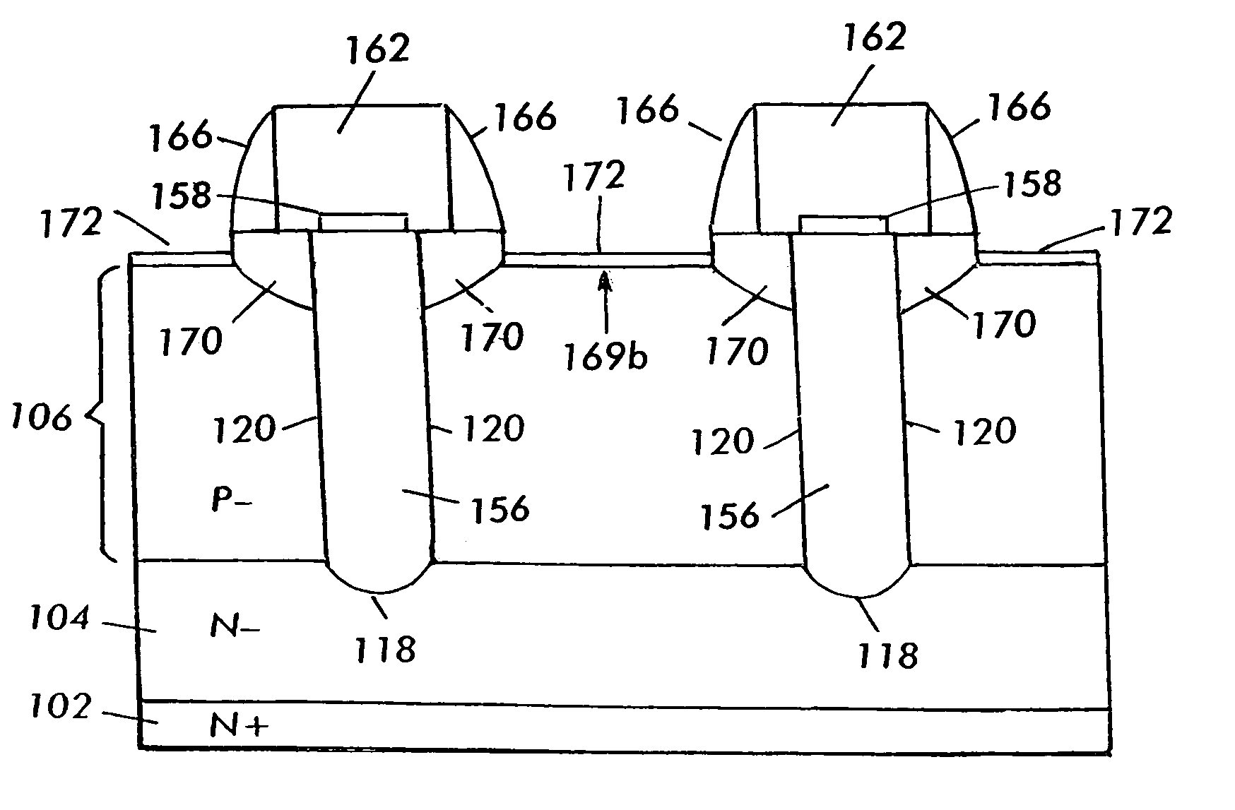
[0010]Accordingly, it would be desirable to produce a trench type power semiconductor device that has increased cell density, thereby overcoming the above and other disadvantages of the prior art. In accordance with the present invention, power MOSFETs are fabricated through the use of inside and outside spacers that allow for the formation of gate electrode trenches with reduced widths and also allow for the self-alignment of source regions and high conductivity contact regions between each other and the trenches, which in turn allows for reduced distances between trenches. In accordance with a further aspect of the invention, shallower source regions are obtained. At least one benefit of these shallower source regions is that there is less lateral diffusion of the regions, thereby again allowing for reduced distances between trenches. As a result, power MOSFETs fabricated according to the present invention have reduced cell pitch and increased cell density. In general, the fabrication process of the present invention is applicable to power MOSFETS that have gate electrodes recessed below the top surface of the semiconductor body and to power MOSFETS that have gate electrodes that extend above the top surface of the semiconductor body.
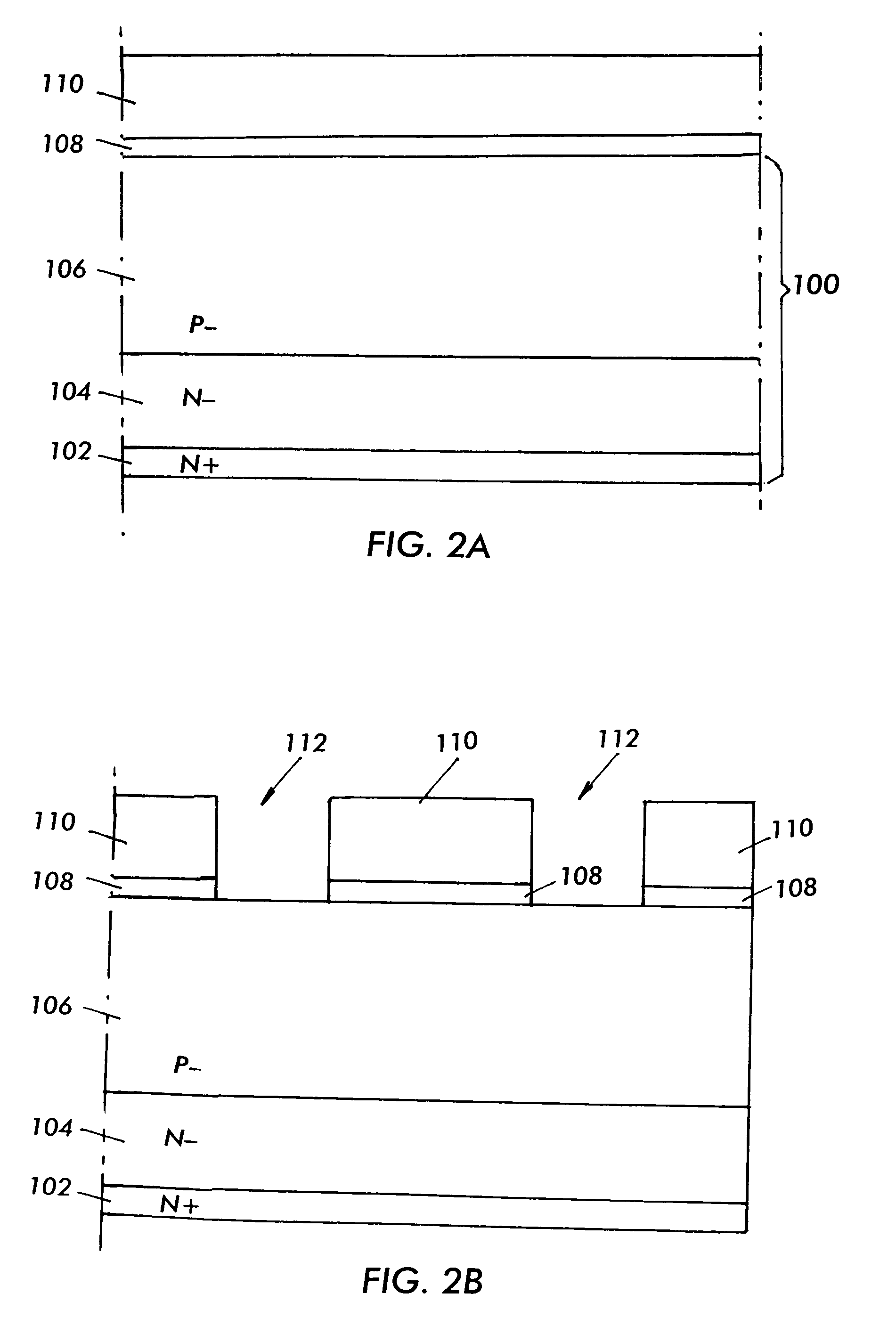
[0011]More specifically, in accordance with a first embodiment of the present invention, a hard mask layer is first formed over the surface of a semiconductor body, which includes a substrate and epitaxial silicon layer of a first conductivity and a channel region thereupon of a second conductivity. This mask layer is then etched to form a plurality of openings that extend to and expose the surface of the semiconductor body. Inside spacers are then formed along the sidewalls of these openings such that the spacers expose a defined area of the surface of the semiconductor body. Using these spacers as masks, gate electrode trenches are formed into the channel region and epitaxial silicon layer of the semiconductor body. Notably, the use of the inside spacers to create the trenches allows for the formation of narrower trenches than a process such as photo-lithography, for example, would permit.
[0013]Next, the inside spacers are removed and source implant regions are formed in the channel region along the upper edges of the trenches. A diffusion drive is then carried out to form source regions. Notably, through the use of the inside spacers, the source regions are formed through self-alignment, thereby eliminating a need for a mask.
[0015]Using the outside spacers as masks, a contact etch is next performed along the surface of the semiconductor body and high conductivity contact regions are formed therein. The outside spacers are then removed and source and drain contacts formed. Notably, through the use of the outside spacers, the high conductivity contact regions are self-aligned between adjacent source regions and adjacent gate electrode trenches. Overall, by using the inside and outside spacers to self-align the source regions and high conductivity contact regions between each other and the gate electrode trenches, the distance between adjacent trenches can be reduced.
[0016]In accordance with a second embodiment of the invention, a two-phase source implant is used that results in shallower source regions as compared to the first embodiment. As indicated, shallower source regions result in less lateral diffusion of the source implants, which allows for the distance between adjacent trenches to be reduced, among other benefits.

Problems solved by technology

However, traditional fabrication processes can limit the amount of reduction in these dimensions.
For example, traditional masking methods used during the fabrication of a power MOSFET make it difficult to reduce trench width.
Similarly, traditional masking methods can lead to mask misalignments.
However, increased sizes lead to larger distances between trenches.

Method used


Image

  • Trench power MOSFET fabrication using inside/outside spacers
  • Trench power MOSFET fabrication using inside/outside spacers
  • Trench power MOSFET fabrication using inside/outside spacers

Examples


first embodiment

[0023]Referring to FIGS. 2A-2L (note that the Figures are not drawn to scale), a power MOSFET fabrication process according to the invention is illustrated, the fabrication process here resulting in gate electrodes that are recessed below the top surface of the semiconductor body. Beginning with FIG. 2A, there is shown an initial silicon body 100. Silicon body 100 preferably includes a silicon substrate 102 of one conductivity (e.g., N-type) and epitaxial silicon layer 104 of the same conductivity (e.g., N-type) grown over one major surface of silicon substrate 102. As is known, epitaxial silicon layer 104 includes a lower concentration of dopants as compared to substrate 102. Silicon body 100 also includes channel region 106, which has conductivity opposite to that of epitaxial silicon layer 104 (e.g. P-type). Preferably, channel region 106 is formed by implanting dopants on the surface of silicon layer 104 and driving these dopants in a diffusion drive to a desired channel depth. ...

second embodiment

[0042]Referring to FIG. 4B, inside spacers 114 are next removed exposing a portion of channel region 108 along the upper edges of each trench 118. The process then proceeds similar to the second embodiment for the formation of the source regions. Specifically, a first source implant is next carried out to form source implant regions 160 in channel region 106 along the upper edges of each trench 118. However, again, a source diffusion drive is not carried out. Rather, a layer of oxide, composed from TEOS or the like for example, is formed over the surface of the structure, covering hard mask layer 110 and filling openings 112. This oxide layer is then etched back, forming insulation caps 162 over the gate electrodes 156. The resulting structure is shown in FIG. 4B.

[0043]Referring to FIG. 4C, an appropriate etching process is next carried out to remove the remaining hard mask layer 110 and pad oxide layer 108. As a result, openings 134 are formed between adjacent insulation caps 162, ...


PUM


Abstract

A fabrication process for a trench type power semiconductor device includes forming inside spacers over a semiconductor surface. Using the spacers as masks, trenches with gates are formed in the semiconductor body. After removing the spacers, source implants are formed in the semiconductor body along the trench edges and are then driven. Insulation caps are then formed over the trenches. Outside spacers are next formed along the sides of the caps. Using these spacers as masks, the semiconductor surface is etched and high conductivity contact regions formed. The outside spacers are then removed and source and drain contacts formed. Alternatively, the source implants are not driven. Rather, prior to outside spacer formation a second source implant is performed. The outside spacers are then formed, portions of the second source implant etched, any remaining source implant driven, and the contact regions formed. The gate electrodes are either recessed below or extend above the semiconductor surface.

Description

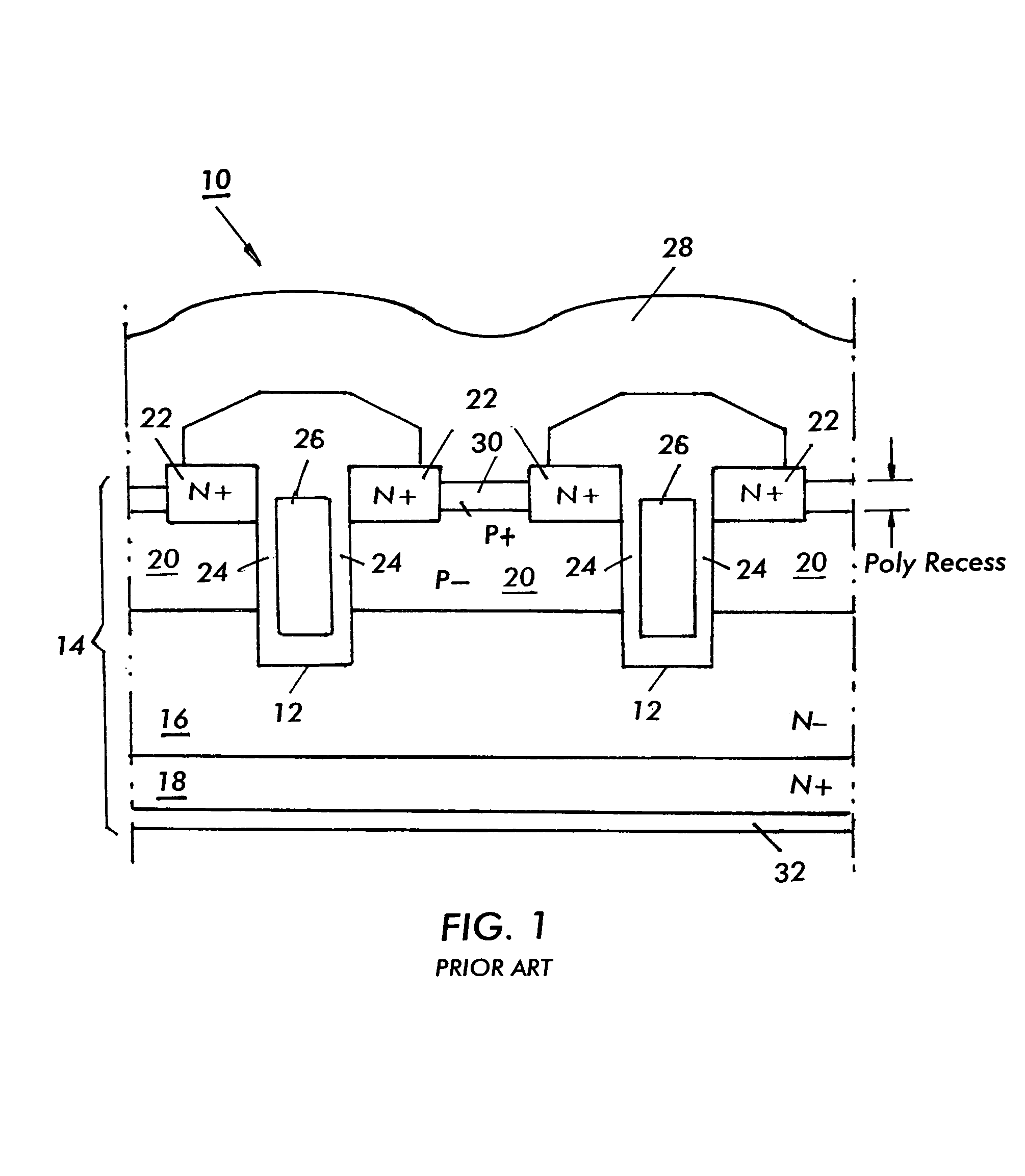
RELATED APPLICATIONS[0001]This application is based on and claims priority to U.S. Provisional Application No. 60 / 543,164, filed on Feb. 9, 2004, by Robert Montgomery, entitled, “Trench FET with Inside / Outside Spacer and Single Source,” to U.S. Provisional Application No. 60 / 543,143, filed on Feb. 9, 2004, by Kyle Spring, entitled, “Trench FET with Inside / Outside Spacer and Double Source,” and to U.S. Provisional Application No. 60 / 543,441, filed on Feb. 9, 2004, by Jianjun Cao, Paul Harvey, David Kent, Robert Montgomery, and Kyle Spring, entitled, “Trench Power MOFET with Reduced Gate Resistance,” the contents of which are herein incorporated by reference.BACKGROUND OF THE INVENTION[0002]1. Field of the Invention[0003]The present invention relates generally to MOSFET fabrication, and more specifically, to MOSFET fabrication that uses spacers as masks.[0004]2. Description of Related Art[0005]Trench type power semiconductor devices such as power MOSFETs are well known. Referring to F...

Claims


Application Information

Patent Timeline
Patent Type & Authority Patents(United States)
IPC IPC(8): H01L21/8242H01L21/20H01L21/336H01L29/45H01L29/49H01L29/78
CPCH01L29/66719H01L29/66727H01L29/66734H01L29/7813H01L29/456H01L29/4933
Inventor CAO, JIANJUNHARVEY, PAULKENT, DAVIDMONTGOMERY, ROBERTSPRING, KYLE
Owner INFINEON TECH AMERICAS CORP
Learn More