Image sensor module
a technology of image sensor and module, which is applied in the field can solve the problems of high manufacturing cost of image sensor module, inability to obtain clear images, and inability to achieve clear images, etc., and achieve the effect of facilitating accurate mounting of lenses
- Summary
- Abstract
- Description
- Claims
- Application Information
AI Technical Summary
Benefits of technology
Problems solved by technology
Method used
Image

Examples
first embodiment
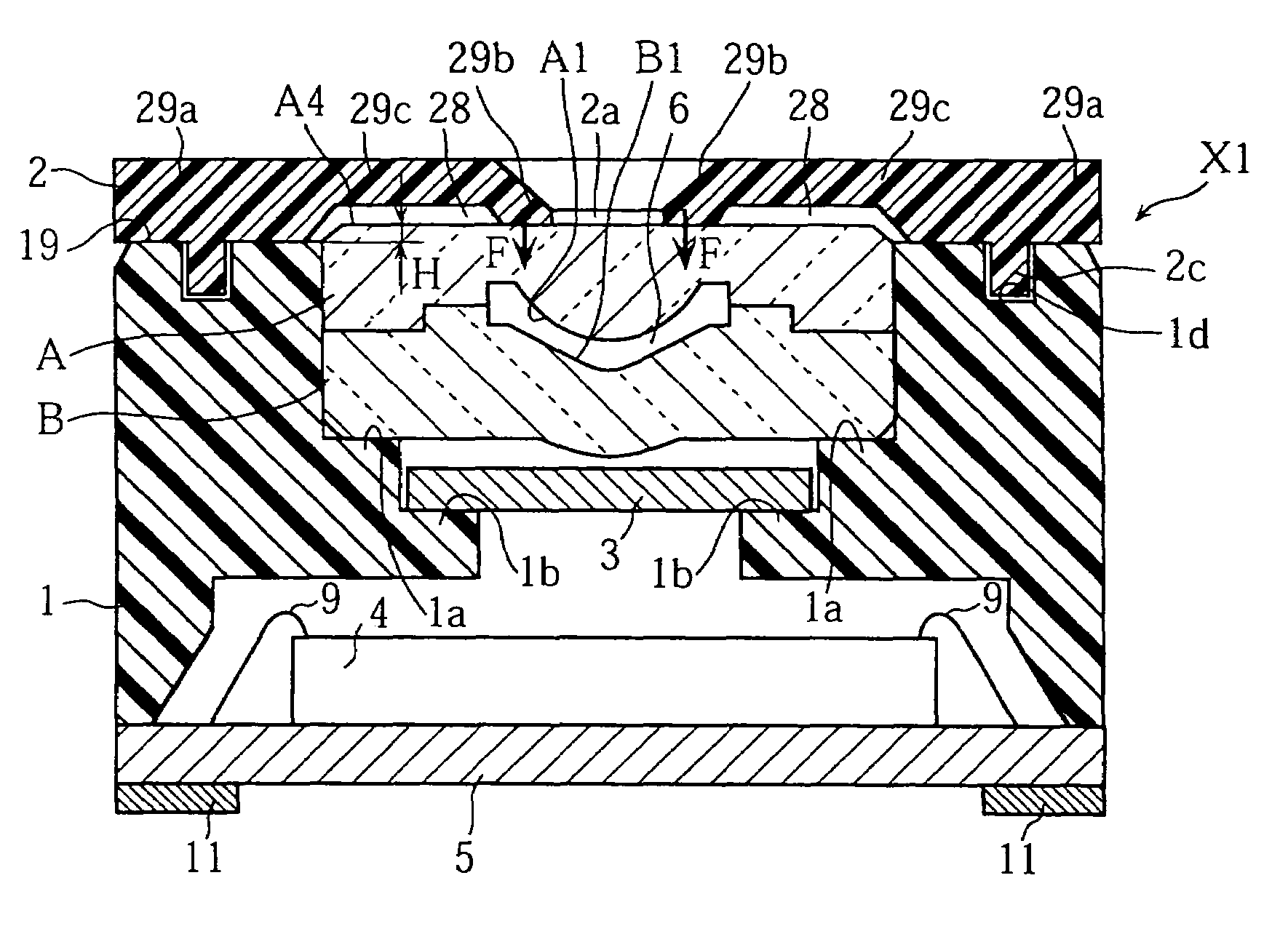
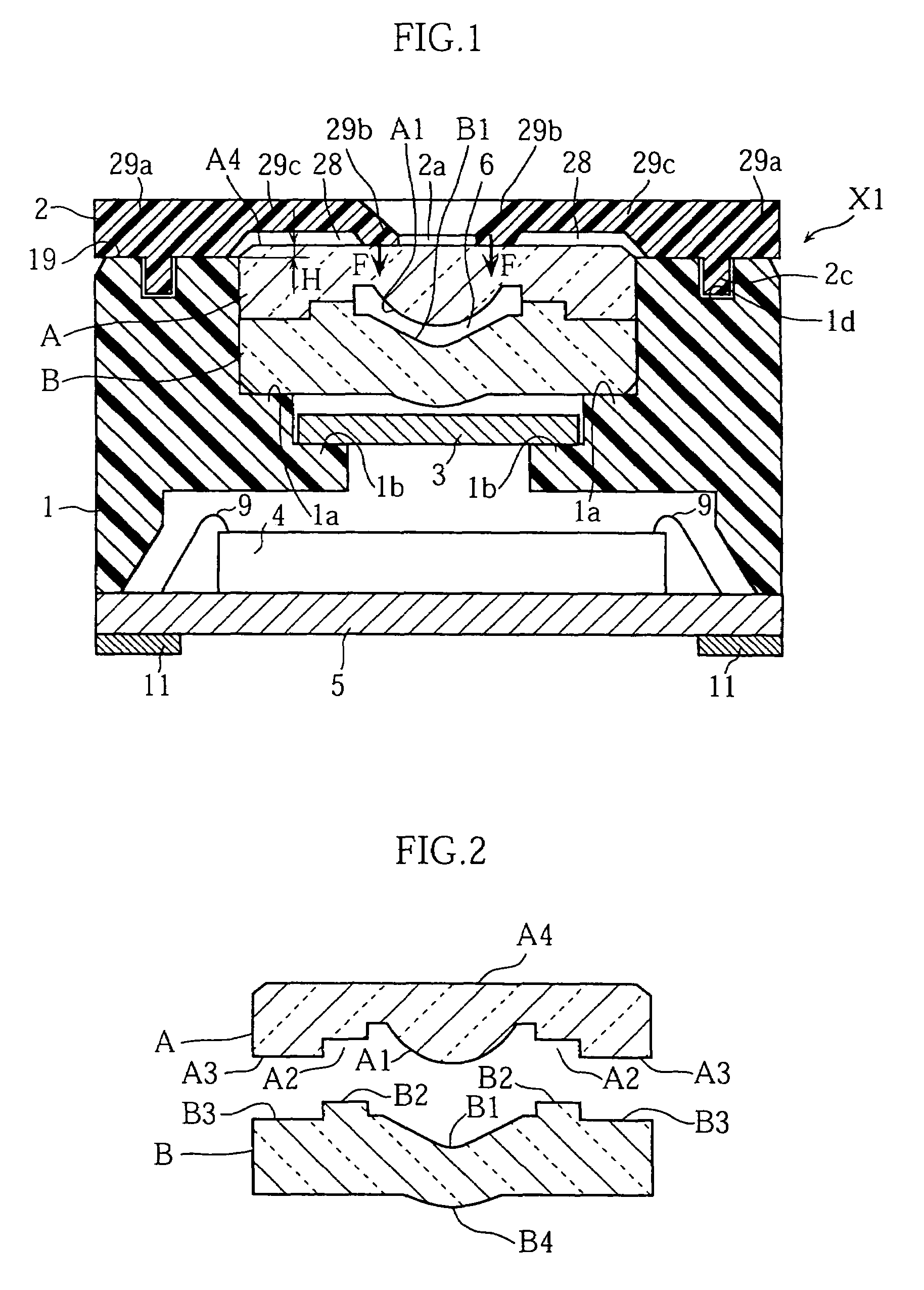
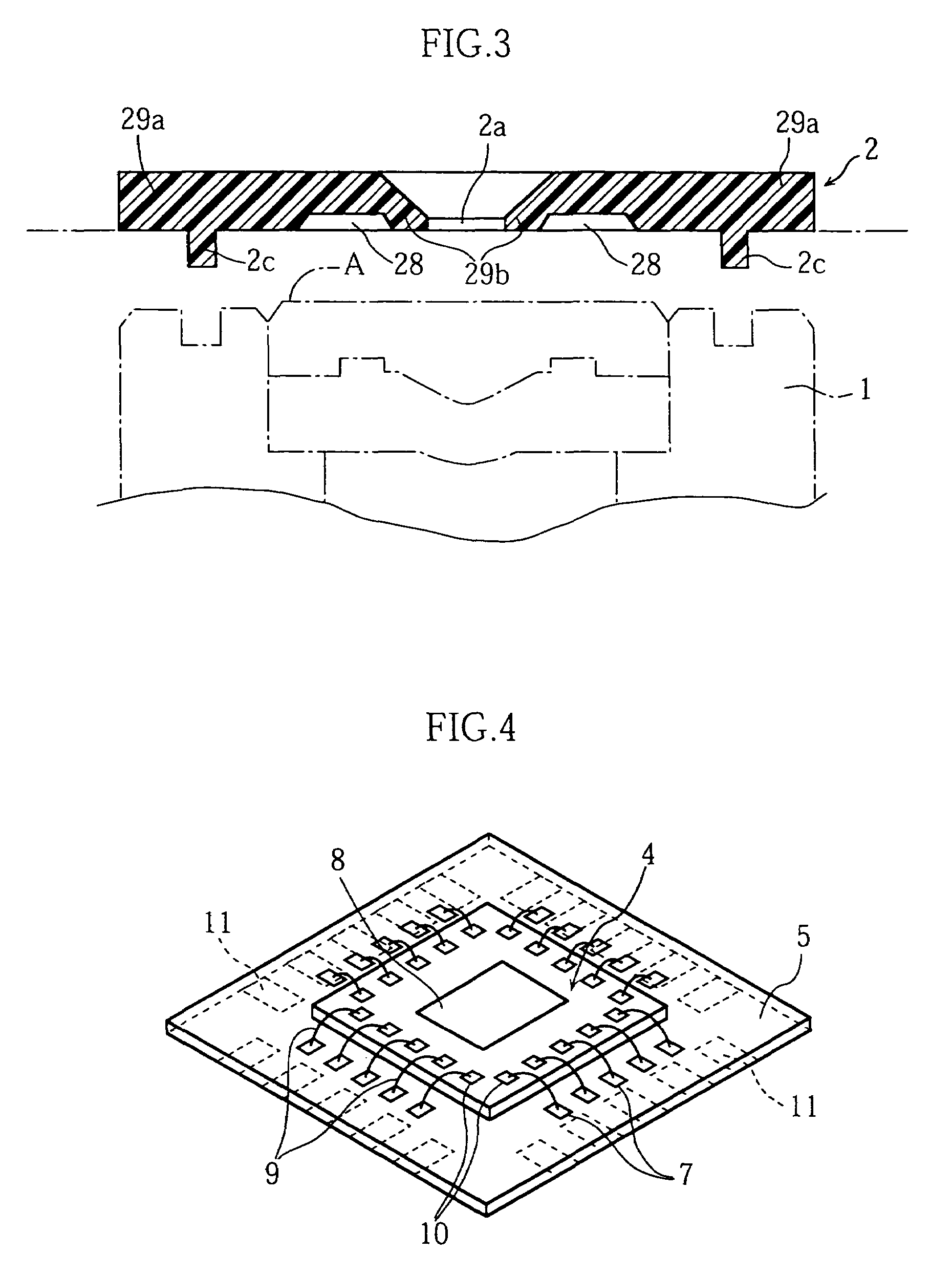
[0040]FIG. 1 shows an image sensor module X1 according to the present invention. The image sensor module X1 comprises first and second lenses A and B, a housing 1, a lens retainer 2, an optical filter 3, an image sensor chip 4 and an insulating substrate 5.
[0041]The substrate 5 is a rectangular plate. The image sensor chip 4 is a CCD type or a CMOS type solid image sensing device, and is mounted on the substrate 5. As FIG. 4 shows, the image sensor chip 4 comprises a light receiving section 8 for receiving light, a plurality of electrodes 10 and a photo-electric conversion section (not illustrated) which is built inside. The light received by the light receiving section 8 is converted into electric charges corresponding to the received light quantity by the photo-electric conversion section. The electric charges are output from the electrodes 10. The electrodes 10 are connected to a plurality of conductor pads 7 formed on the surface of the substrate 5 via wires 9. A plurality of te...
third embodiment
[0055]An image sensor module (X3: see FIG. 8) according to the present invention will now be described with reference to FIG. 6 to FIG. 8.
[0056]In the first and second embodiments, the lens unit is accurately positioned by using the biasing force of the lens retainer 2. However, if the following method is used, the lens unit can be accurately positioned with respect to the image sensor chip without using such a lens retainer.
[0057]As FIG. 6 shows, the module according to the third embodiment includes a housing 1, which is similar to the housing shown, in FIG. 5. The housing 1 fixedly receives an optical filter 3 together with first and second lenses A and B. The upper face of the first lens A is provided with a diaphragm 13. The diaphragm 13 is provided with an opening 13a for transmitting light. The unit shown in FIG. 6 will be referred to as “lens assembly” herein below.
[0058]As FIG. 7 shows, the lens assembly is fixed to the substrate 5 by using the handling device 14 as follows....
fifth embodiment
[0073]FIG. 12 shows an image sensor module X5 according to a The image sensor module X5 comprises an image sensor chip 1′, a substrate 2′ on which the image sensor chip 1′ is mounted, a lens unit 3′, a diaphragm 4′ disposed on the lens unit 3′, an optical filter 5′ disposed on the diaphragm 4′, and a housing 6′ surrounding the lens unit 3′. The lens unit 3′ is a combination of the first and second lenses 31, 32.
[0074]The image sensor chip 1′ is a CCD type or CMOS type solid image sensing device. The upper face of the image sensor chip 1′ is centrally provided with a light receiving section 11′ for receiving light which transmits through the lens unit 3′. The image sensor chip 1′ is electrically connected to lands (not illustrated) on the substrate 2′ via a plurality of wires 12′. The image sensor chip 1′ outputs signals to the outside via the wires 12′ according to the quantity of light received by the light receiving section 11′. The output signals are used as pixel information vi...
PUM
 Abstract
Description
Claims
Application Information
 - R&D
- Intellectual Property
- Life Sciences
- Materials
- Tech Scout
- Unparalleled Data Quality
- Higher Quality Content
- 60% Fewer Hallucinations
Browse by: Latest US Patents, China's latest patents, Technical Efficacy Thesaurus, Application Domain, Technology Topic, Popular Technical Reports.
© 2025 PatSnap. All rights reserved.Legal|Privacy policy|Modern Slavery Act Transparency Statement|Sitemap|About US| Contact US: help@patsnap.com