Method of mounting semiconductor chip

Inactive Publication Date: 2008-07-01
FUJITSU LTD
View PDF18 Cites 6 Cited by
  • Summary
  • Abstract
  • Description
  • Claims
  • Application Information

AI Technical Summary

Benefits of technology

[0029]Since the peripheral portion of the insulating adhesive spread out between the semiconductor chip and the substrate while the semiconductor chip is pressed, a large amount of overflow of the insulating adhesive can be prevented. Thus, the fillet of the underfill can be formed in a preferable shape.
[0048]When the bonding tool applies ultrasonic oscillation to the semiconductor chip, the semiconductor chip tends to be displaced due to the orientation of the bonding tool. In the above configuration, however, the bumps formed on the semiconductor chip do not move off the pads each having a shape elongated in the direction of the ultrasonic oscillation. Thus, defective bonding can be prevented between the semiconductor chip and the substrate.

Problems solved by technology

1. The shape of the fillet of the underfill is unstable.
Furthermore, the large amount of overflow of the adhesive has an adverse effect on the on the floating characteristic of the head slider 20 with respect to a hard disk.
However, it is troublesome to clean the top end of the tool 75 every time the mounting of one head IC chip 11 is completed.
4. The head IC chip often deviates at the time of mounting, and the deviation results in defective mounting.

Method used


Image

  • Method of mounting semiconductor chip
  • Method of mounting semiconductor chip
  • Method of mounting semiconductor chip

Examples


first embodiment

[0086]The first embodiment solves the problem that the shape of the fillet of the underfill is insecure.

[0087]FIGS. 9A and 9B show a head IC chip mounting device 100 as a first embodiment of the present invention. The head IC chip mounting device 100 comprises a stage 101, a bonding unit 110, and a control unit 130.

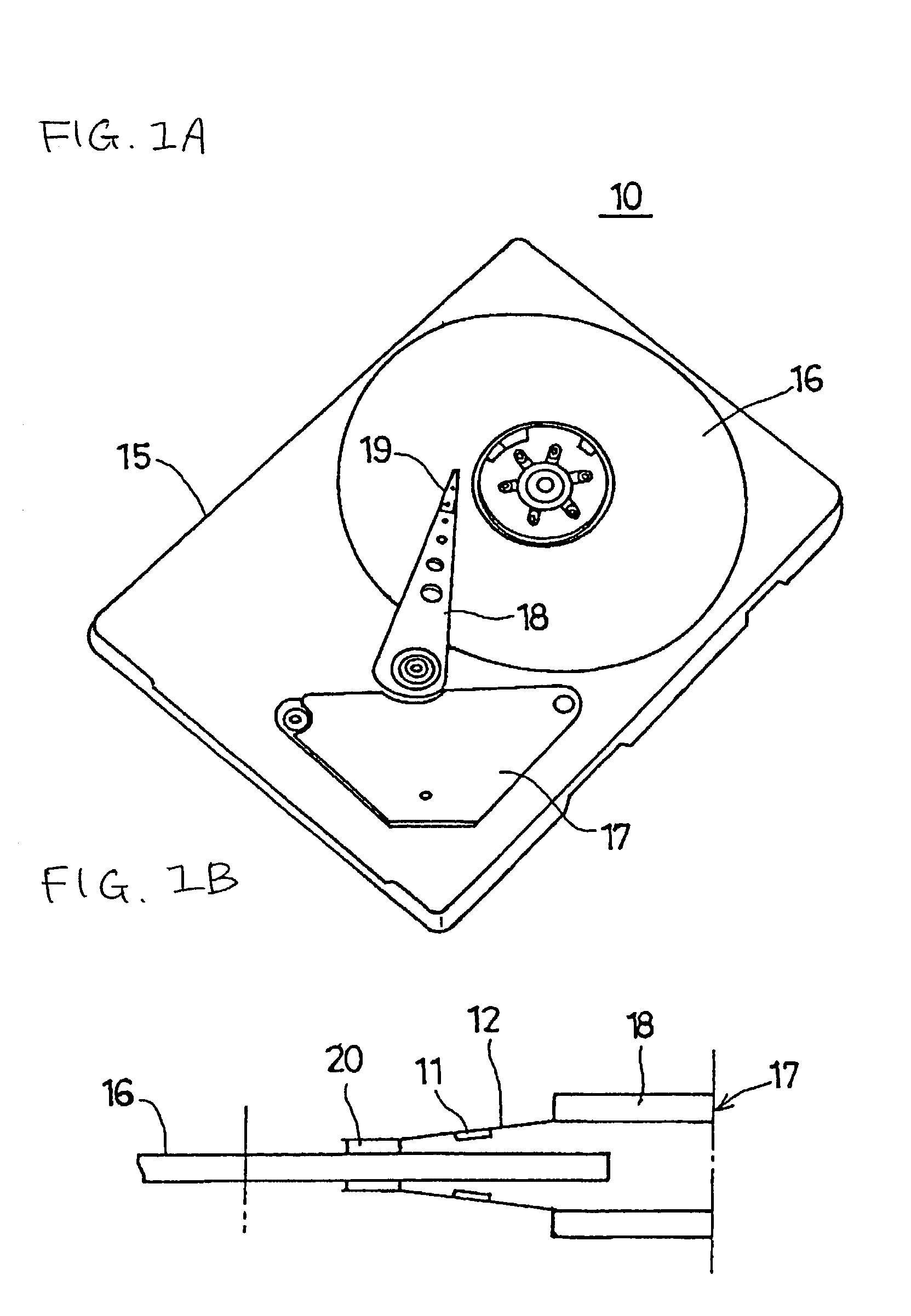
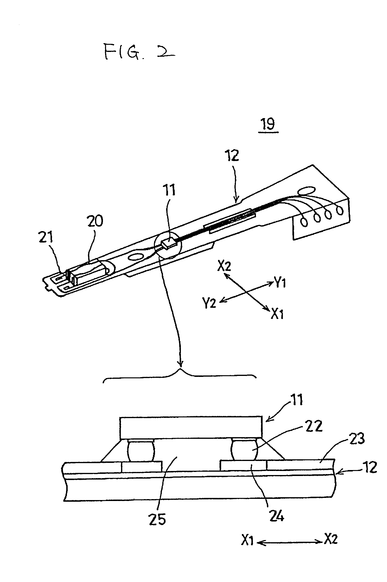
[0088]The stage 101 accommodates the suspension 12 shown in FIG. 2, and is provided with suction holes 102 for sucking and attracting the suspension 12. Also on the stage 101, four. ultraviolet lamps 104 to 107 surround a chip mounting position 109, and face the four sides of a mounted head IC chip 11 so as to irradiate all the four sides of the head IC chip 11 with ultraviolet rays.

[0089]The bonding unit 110 comprises a bonding head 111, a bonding tool 112 hanging from the bonding head 111, and an ultrasonic oscillator 113 integrally formed with the bonding tool 112. The bonding tool 112 is moved up and down by an elevating mechanism (not shown). The bonding unit 110 is ...

second embodiment

[0117]FIGS. 18A and 18B illustrate a chip mounting device 100 of the present invention. The chip mounting device 100A is provided with heaters 164 to 167 in place of the ultraviolet lamps 104 to 107 of the chip mounting device 100 shown in FIGS. 9A and 9B. The heaters 164 to 167 surround the chip mounting position 109, and are arranged so as to irradiate all the sides of the head IC chip 11 with thermal rays 168.

[0118]As for the adhesive, thermosetting adhesive 150A is used.

[0119]When the head IC chip 11 is pressed against the suspension 12 and when the head IC chip 11 is subjected to an ultrasonic wave, the heaters 164 to 167 are switched on to irradiate the portion 151a of the thermosetting adhesive 150A exposed out of the rim of the head IC chip 11 with the thermal rays 168, thereby hardening the exposed portion 151a. Thus, the adhesive 150A can be prevented from flowing out of the suspension 12, and an excellent fillet 156 can be formed.

[0120]Third, fourth and fifth embodiments ...

third embodiment

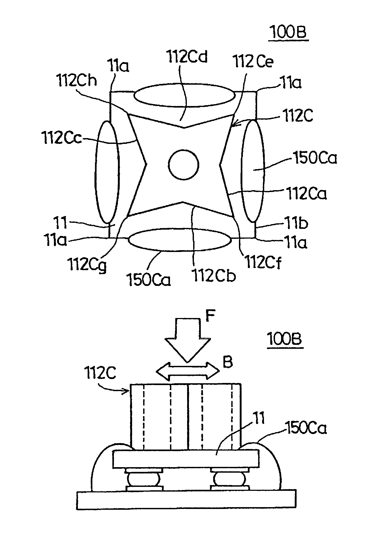
[0121]FIGS. 19A and 19B illustrate a chip mounting device 100B of the present invention. The chip mounting device 100B does not include the ultraviolet lamps 104 to 107 and the controller 134 of the chip mounting device 100 shown in FIGS. 9A and 9B, and is provided with a bonding tool 112C shown in FIG. 20 instead of the bonding tool 112.

[0122]The bonding tool 112C is made of stainless steel, and takes the form of a pillar. The section of the bonding tool 112C has a square shape corresponding to the shape of the head IC chip 11. Also, the bonding tool 112C is the same size as the conventional bonding tool 112. The bonding tool 112C differs from the bonding tool 112 in that it has V-shaped sides. In other words, the bonding tool 112C is basically a square pole having four V-shaped side surfaces 112Ca to 112Cd and four corners 112Ce to 112Ch. The side surfaces 112Ca to 112Cd are bent inward with respect to the virtual flat surfaces between every two adjacent corners of the corners 112...


PUM

PropertyMeasurementUnit
Shapeaaaaaaaaaa
Friction coefficientaaaaaaaaaa

Abstract

A method of mounting a semiconductor chip in which an IC chip is mounted by filling a gap between the chip and a substrate with adhesive which functions as an underfill. The fillet of the underfill is made to have a preferable shape. To accomplish this, a head IC chip provided with bumps is placed on a suspension that is covered with the underfill adhesive and is provided with pads. A bonding tool presses the head IC chip and applies ultrasonic oscillation to the head IC chip, so that the bumps are properly bonded to the pads. When the head IC chip is pressed and subjected to ultrasonic oscillation, the ultraviolet rays 108 are emitted so as to harden the peripheral portion 151a of the adhesive 151 spread out between the head IC chip 11 and the suspension 12.

Description

[0001]This application is a divisional of prior application Ser. No. 09 / 614,726 filed Jul. 12, 2000 now U.S. Pat. No. 6,437,450.BACKGROUND OF THE INVENTION[0002]1. Field of the Invention[0003]The present invention generally relates to a method of mounting a semiconductor chip and an apparatus for mounting a semiconductor chip.[0004]The method of mounting a semiconductor chip can be applied to mounting of a head IC chip 11 of a hard disk device 10 to a suspension 12, as shown in FIGS. 1A and 1B, or to mounting of an IC chip 31 of a printed circuit board unit 30 to a substrate 32, as shown in FIGS. 3A to 3C.[0005]As shown in FIGS. 1A and 1B, the hard disk device 10 has a hard disk 16 that rotates at high speed in a hermetically sealed housing 15, and a head slider assembly 19 attached to the top end of an arm 18. The head slider assembly 19 comprises a head slider 20 and the head IC chip 11 mounted on the suspension 12, as shown in FIG. 2. The head slider 20 has a magnetic head 21 for...

Claims


Application Information

Patent Timeline
IPC IPC(8): H01L23/48H01L23/52H01L29/40H01L23/28G11B5/60G11B21/21H01L21/00H01L21/56H01L21/60H01L21/607H01L23/29H01L23/31H05K3/32
CPCH01L21/563H01L21/67092H01L24/83H01L24/29H01L21/67144H01L24/32H01L24/75H01L2924/07802H01L2224/81191H01L2924/10253H01L2924/01023H01L2924/01006H01L2224/32225H01L2924/14H01L2924/01082H01L2924/01079H01L2924/01039H01L2924/01033H01L2924/01029H01L2924/01005H01L2924/01004H01L2224/85444H01L2224/83951H01L2224/83885H01L2224/83874H01L2224/83868H01L24/81H01L2224/1134H01L2224/13144H01L2224/16225H01L2224/48227H01L2224/73203H01L2224/73204H01L2224/75H01L2224/75743H01L2224/81205H01L2224/81801H01L2224/83192H01L2224/83859H01L2224/83862H01L2924/00H01L2924/00012H01L2924/3512H01L2224/05573H01L2224/05568H01L2924/00014H01L2224/05599
Inventor BABA, SHUNJIYAMAKAMI, TAKATOYOKAINUMA, NORIOKOBAE, KENJIKIRA, HIDEHIKOKOBAYASHI, HIROSHI
Owner FUJITSU LTD
Why Eureka
Try Eureka