Sensor arrangement with a plurality of potentiometric sensors

a potentiometric and sensor technology, applied in the direction of resistance/reactance/impedence, instruments, material electrochemical variables, etc., can solve the problems of complex solutions, high cost, and complicated solutions proposed by benton, and achieve safe and secure housing, ensure electrical conductivity, and optimize the sealing effect of elastic layers

Inactive Publication Date: 2008-07-01
ENDRESS HAUSER CONDUCTA GESELLSCHAFT FUER MESS UND REGELTECHNIK MBH CO KG
View PDF8 Cites 158 Cited by
  • Summary
  • Abstract
  • Description
  • Claims
  • Application Information

AI Technical Summary

Benefits of technology

[0012]The FET-sensors, which can be present, for example, as separate chips or as a plurality of sensor elements in an, as required, monolithic floor element, have, in order to implement a sensor, to be arranged in such a manner that they, on the one hand, can be contacted by the possibly corrosive samples, without that, on the other hand, corrosion-sensitive components, e.g. conductive traces, come in contact with the media. To this end, an embodiment of the invention provides that FET-sensors are arranged in such a manner that the ion-sensitive surface regions of the FET-sensors align with bores of the sample chambers, with a ring-shaped seal being arranged between the platform and the FET-sensors. The seal surrounds the bores, so that the ion-sensitive region of the semiconductor chip can be contacted by the sample, without the sample coming in contact with the FET-sensor outside of the region enclosed by the seal. For the electrical contacting of the FET-sensors, various embodiments are possible.
[0015]To the extent that the elastic layer contains metal grains, these are uniformly distributed in the case of a relaxed layer in such a concentration that there is not a sufficient number of electrical contacts between the grains to produce an electrical conductivity over large distances. If, however, the elastic layer is compressed in some direction, for example by being clamped as a sealing element between the first module and the second module, or between the platform and the floor element, as the case may be, then there arises in the direction of compression a sufficient number of electrical contacts for assuring conductivity along the direction of compression. Independently of the selected type of sealing element, the FET-sensors, or the floor element, can be pressed by a rear-side support against the elastic layer, in order to optimize the sealing effect of the elastic layer. The rear-side support can be both stiff as well as also elastically prestressed. The elastic prestressing, e.g. with a coil spring, is advantageous in the respect that, thereby, the effects of different coefficients of thermal expansion can be safely accommodated, as compared with accomplishing such solely by the elasticity of the sealing element. This is especially important, when a certain degree of compression of the sealing element is required, in order to assure the electrical conductivity through the seal.

Problems solved by technology

The solution proposed by Benton is very complex, to the extent that, both in the case of the manufacture of the seal and also in the case of the implementation of the electrical contacting, involved solder, braze, or weld processes are required.
Also, this solution is complicated, because bonding tasks are required for contacting the chip, and because, for assuring function and integrity of the sensor, the chip must be oriented within narrow tolerances, both with reference to the substrate and with reference to the carrier.
These solutions are very expensive hi-the with respect that to the leading of the electrical contacts through the chip from its front side to its rear side1 makes making its manufacturing costs a number of times greater.

Method used


Image

  • Sensor arrangement with a plurality of potentiometric sensors
  • Sensor arrangement with a plurality of potentiometric sensors
  • Sensor arrangement with a plurality of potentiometric sensors

Examples


Embodiment Construction

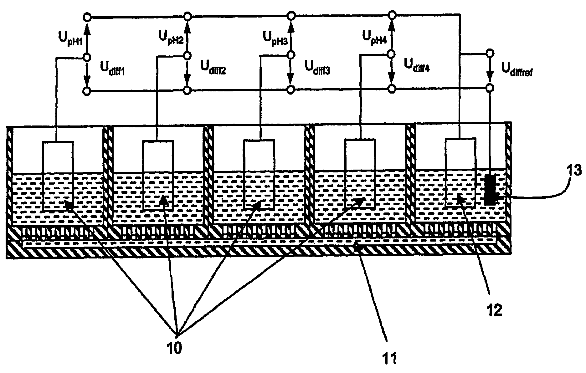
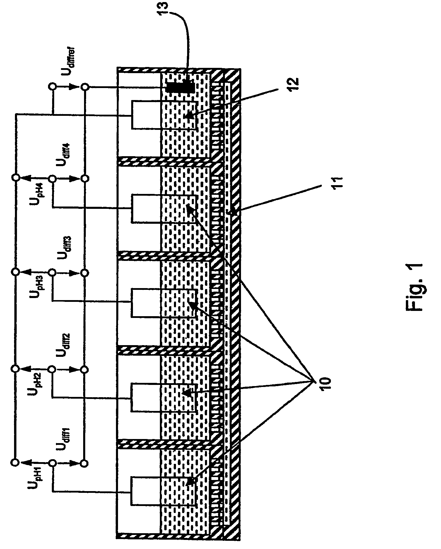
[0021]FIG. 1 shows schematically the principles of functioning of the sensor arrangement of the invention. The FET-sensors 10 of the sensor arrangement have, in each case, a sensitive gate-region, which is contactable with an analyte in a sample chamber. The individual sample chambers of the sensor arrangement are connected with one anther via an electrolyte bridge. To this end, the electrolyte bridge includes an electrolyte canal, which communicates with the sample chambers via diaphragms. The sensor arrangement further includes a reference chamber, in which a reference electrode 13, for example of platinum, and reference-FET 12 are located. The reference-FET outputs a pseudo-reference-potential Udiffref, against which the potentials Udiff1, Udiff2, . . . UdiffN of the N FET-sensors in the sample chambers are measured. The measured-variable-relevant, potential difference, for example UpH1, is determined by forming the difference between the applicable potential and the reference po...


PUM

PropertyMeasurementUnit
pHaaaaaaaaaa
resistancesaaaaaaaaaa
conductiveaaaaaaaaaa

Abstract

The sensor arrangement includes: a least two sample chambers; at least two potentiometric FET-sensors, especially ISFET-sensors or ChemFET-sensors, having, in each case, a sensitive surface section, wherein each sensitive surface section lies in flow connection with its one of the sample chambers; and a reference cell having a reference medium for providing a reference potential, wherein the sample chambers are connected with the reference medium via an electrolyte bridge. The reference cell has, preferably, a potentiometric reference-FET-sensor for providing a reference potential, which is registered against the pseudo-reference-potential of a redox electrode. The potentials Udiff1, Udiff2, . . . UdiffN of N FET-sensors in the sample chambers are determined against the pseudo-reference-potential, and the measured-variable-relevant, potential differences are determined, in each case, by difference formation between the pertinent potential and the reference potential—thus, in the case of pH, according to the formulasUpH1. . . N=Udiff1. . . N−Udiffref.

Description

FIELD OF THE INVENTION[0001]The present invention relates to a sensor arrangement for the potentiometric testing of a plurality of samples, especially such an arrangement having so-called ISFET or CHEMFET sensors.BACKGROUND OF THE INVENTION[0002]These kinds of potentiometric FET-sensors are suited for measuring the pH value or the redox potential of an analyte. DE 198 57 953 C2 concerns, for example, the realization of a pH-ISFET-sensor, in which, for reducing the circuit complexity, the ISFET-sensor is connected in a bridge circuit having at least three additional resistances. Regarding the mounting of the FET-sensor, the following principles are, among others, known. Benton discloses in U.S. Pat. No. 5,833,824 a pH-sensor, in which an ISFET-chip is secured on the underside of a substrate by means of a metal seal, which surrounds the ion-sensitive region of the ISFET-chip, with the ion-sensitive region being aligned with an opening in the substrate. Outside of the region surrounded...

Claims


Application Information

Patent Timeline
Patent Type & Authority Patents(United States)
IPC IPC(8): G01R27/00G01N27/414
CPCG01N27/414
Inventor PECHSTEIN, TORSTENBABEL, WOLFGANGSTECKENREITER, THOMAS
Owner ENDRESS HAUSER CONDUCTA GESELLSCHAFT FUER MESS UND REGELTECHNIK MBH CO KG
Why Eureka
Try Eureka