Semiconductor device having a dual gate electrode and methods of forming the same

a technology of semiconductor devices and gate electrodes, which is applied in semiconductor devices, lighting and heating devices, domestic cooling devices, etc., can solve the problems of less effective fermi pinning effect provided to the first gate electrode than that provided to the second gate electrode, and achieve the effects of reducing intrinsic work functions, increasing intrinsic work functions, and reducing silicon concentration

Active Publication Date: 2008-07-08
SAMSUNG ELECTRONICS CO LTD
View PDF8 Cites 15 Cited by
  • Summary
  • Abstract
  • Description
  • Claims
  • Application Information

AI Technical Summary

Benefits of technology

[0010]In one aspect, the present invention is directed to a semiconductor device. The device includes a substrate having first and second regions. A first gate electrode made of a first metal silicide is disposed on the substrate in the first region. A second gate electrode made of a second metal silicide including a metal the same as the metal of the first metal silicide is disposed on the substrate in the second region. A gate insulating layer is interposed between the substrate and the first gate electrode, and between the substrate and the second gate electrode. The gate insulating layer brings about a Fermi pinning effect for increasing or decreasing intrinsic work functions of the first and second metal silicides. In this case, the first metal silicide has a lower silicon concentration than the second metal silicide so that the Fermi pinning effect provided to the first gate electrode is less effective than that provided to the second gate electrode.
[0012]In another embodiment, the first region is a region in which an NMOS transistor is formed, and the second region is a region in which a PMOS transistor is formed. Preferably, the gate insulating layer brings about a Fermi pinning effect for increasing intrinsic work functions of the first and second metal silicides. Also, an intrinsic work function of a metal included in the first and second metal silicides is smaller than that of the first and second metal silicides. In this case, it is preferable that the metal included in the first and second metal silicides be one of tantalum and molybdenum. Also, the gate insulating layer bringing about the Fermi pinning effect for decreasing the work function includes at least one of aluminum oxide and aluminum silicate.
[0014]In another aspect, the present invention is directed to a method of forming a semiconductor device. According to the method, a substrate including first and second regions is provided, and a gate insulating layer is formed on a surface of the substrate. A first gate electrode made of a first metal silicide is formed on the gate insulating layer of the first region. A second gate electrode made of a second metal silicide including a metal the same as that of the first metal silicide is formed on the gate insulating layer of the second region. The gate insulating layer is formed of an insulating material bringing about Fermi pinning effect for increasing or decreasing an intrinsic work function of the first and second metal silicides. The first metal silicide has a lower silicon concentration than the second metal silicide so that the Fermi pinning effect provided to the first gate electrode is less effective than that provided to the second gate electrode.
[0016]In another embodiment, the first region is a region in which an NMOS transistor region is formed, and the second region is a region in which a PMOS transistor region is formed. Preferably, the gate insulating layer is formed of an insulating material bringing about Fermi pinning effect for increasing intrinsic work functions of the first and second metal silicides. In this embodiment, an intrinsic work function of a metal included in the first and second metal silicides is smaller than that of the first and second metal silicides.

Problems solved by technology

In this case, the first metal silicide has a lower silicon concentration than the second metal silicide so that the Fermi pinning effect provided to the first gate electrode is less effective than that provided to the second gate electrode.

Method used


Image

  • Semiconductor device having a dual gate electrode and methods of forming the same
  • Semiconductor device having a dual gate electrode and methods of forming the same
  • Semiconductor device having a dual gate electrode and methods of forming the same

Examples


Embodiment Construction

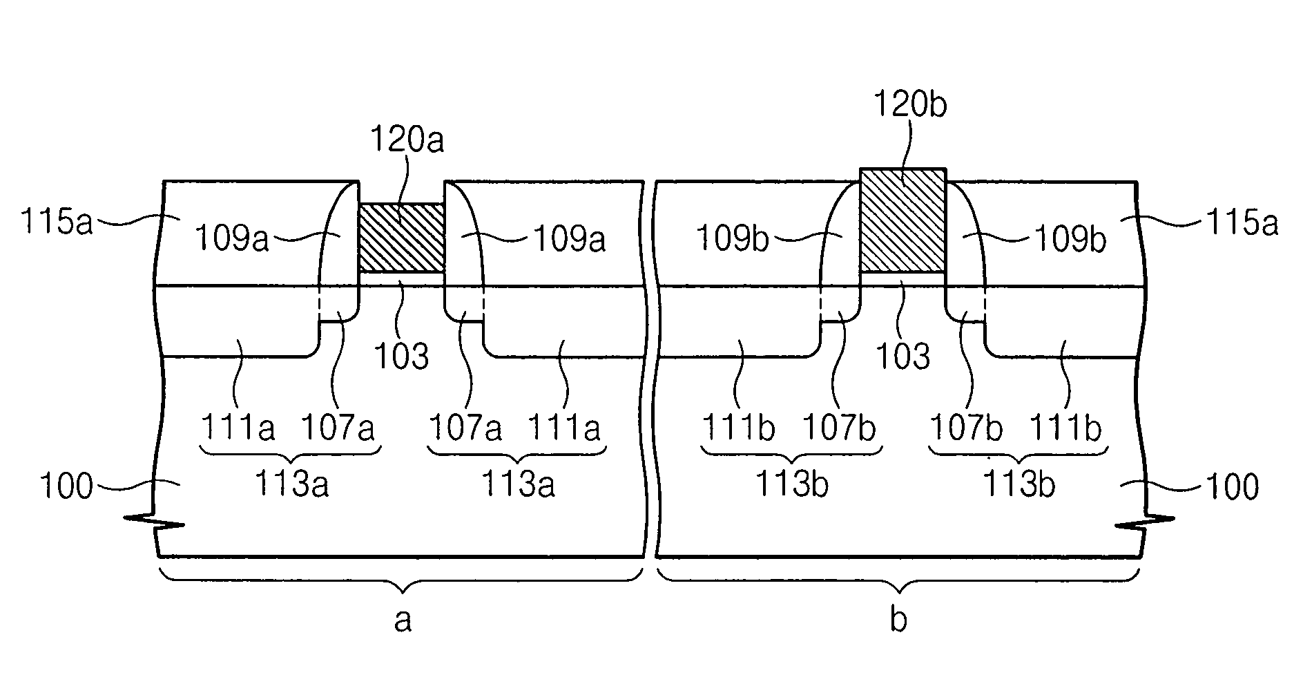
[0024]FIG. 1 is a cross-sectional view showing a semiconductor device according to an embodiment of the present invention. FIG. 2 is a cross-sectional view showing an embodiment of the present invention representing a modification of the embodiment of FIG. 1.

[0025]Referring to FIG. 1, a substrate 100 has a first region a and a second region b. One of the first and second regions a and b is a region in which an NMOS transistor is formed, and the other is a region in which a PMOS transistor is formed.

[0026]A first gate electrode 120a is disposed on the substrate 100 of the first region a, and a second gate electrode 120b is disposed on the substrate 100 of the second region. A gate insulating layer 103 is interposed between the first gate electrode 120a and the substrate 100, and the second gate electrode 120b and the substrate 100.

[0027]The first gate electrode 120a is formed of a first metal silicide, and the second gate electrode 120b is formed of a second metal silicide. The first...


PUM


Abstract

A semiconductor device having a dual gate electrode and a method of forming the same are provided. The semiconductor device includes a substrate including first and second regions. A first gate electrode formed of a first metal silicide is disposed on the substrate of the first region. A second gate electrode is disposed on the substrate of the second region. The second gate electrode is formed of a second metal silicide including a metal the same as that of the first metal silicide. A gate insulating layer is interposed between the substrate and the first gate electrode, and between the substrate and the second gate electrode. The gate insulating layer brings about a Fermi pinning effect increasing or decreasing intrinsic work functions of the first and second metal silicides. In this case, the first metal silicide is a lower silicon concentration than the second metal silicide so that the Fermi pinning effect provided to the first gate electrode is less effective than that provided to the second gate electrode.

Description

CROSS-REFERENCE TO RELATED APPLICATIONS[0001]This U.S. non-provisional patent application claims priority under 35 U.S.C. § 119 of Korean Patent Application 2005-09147 filed on Feb. 1, 2005, the entire contents of which are hereby incorporated by reference.BACKGROUND OF THE INVENTION[0002]The present invention is concerned with a semiconductor device and a method of forming the same, and more specifically relates to a semiconductor device having a dual gate and a method of forming the same.[0003]In general, a CMOS (Complementary Metal Oxide Silicon) semiconductor device includes an NMOS (N-channel Metal Oxide Silicon) transistor and a PMOS (P-channel Metal Oxide Silicon) transistor. Electrons are accumulated in a channel of the NMOS transistor, and holes are accumulated in a channel of the PMOS transistor.[0004]A method for forming gate electrodes of the NMOS and PMOS transistors with polysilicon doped with n-type impurities is disclosed. In accordance with this method, productivity...

Claims


Application Information

Patent Timeline
Patent Type & Authority Patents(United States)
IPC IPC(8): H01L29/78
CPCH01L21/28097H01L21/823835H01L29/66545H01L29/4975H01L21/823842F25D3/08F25D2303/083
Inventor KIM, WOO-SIK
Owner SAMSUNG ELECTRONICS CO LTD
Why Eureka
Try Eureka