Structure and method of sub-gate and architectures employing bandgap engineered SONOS devices

a sonos device and bandgap engine technology, applied in semiconductor devices, digital storage, instruments, etc., can solve the problems of large vt distribution of erase state, difficult to erase, and high threshold cell charge loss, and achieve excellent charge retention, eliminate inter-floating gate coupling effect, and improve scalability

Active Publication Date: 2008-08-19
MACRONIX INT CO LTD
View PDF65 Cites 25 Cited by
  • Summary
  • Abstract
  • Description
  • Claims
  • Application Information

AI Technical Summary

Benefits of technology

[0015]Advantageously, the BE-SONOS AND array architectures of the present invention provides greater scalability over floating gate and AND type of memory devices. The present invention also advantageously provides a uniform and self-converging channel hole tunneling erase operation. Moreover, the present invention eliminates the inter-floating gate coupling effect. The present invention further provides desirable reliability properties including predictable characteristic of excellent charge retention, predictable number of nearly no erratic bits, and predicable small degradation after program and erase cycles.

Problems solved by technology

However, the hot hole injection causes oxide damage, leading to charge loss in the high threshold cell and charge gain in the low threshold cell.
This difference in erase speed results in a large Vt distribution of the erase state, where some of the cells become hard to erase and some of them are over-erased.
Thus the target threshold Vt window is closed after many program and erase cycles and poor endurance is observed.
This phenomenon will become more serious when the technology keeps scaling down.
Floating gate devices encounter substantial scaling challenges due to inter-floating gate coupling, while nitride trapping device is flexible from such limitations.
These two types of devices have drawbacks.
A Nitride Read-Only Memory device is sensitive to hot-hole induced damages, and a SONOS device suffers from retention problems caused by direct tunneling leakage through the thin tunnel oxide.
However, due to the inter-floating gate coupling effect, the scaling of AND-type floating gate devices is limited.
When the space parameter for the floating gate device is shrunk, a high floating gate coupling effect may cause undesirable and severe disturbance.
The conventional AND-type floating gate device also suffers from tunnel oxide scaling issues and erratic bits where a local defect or trapped charge, in a tunnel oxide can result in the leakage of the charge in the floating gate.
However, these devices all suffer serious charge retention problems.
For a SONOS device, the ultra-thin tunnel oxide is unable to properly preserve a charge storage.
For a MNOS device, the structure does not provide a top oxide to block the charge loss.
A nano-crystal device cannot be well-controlled because of the randomly distributed nano particles.

Method used


Image

  • Structure and method of sub-gate and architectures employing bandgap engineered SONOS devices
  • Structure and method of sub-gate and architectures employing bandgap engineered SONOS devices
  • Structure and method of sub-gate and architectures employing bandgap engineered SONOS devices

Examples


first embodiment

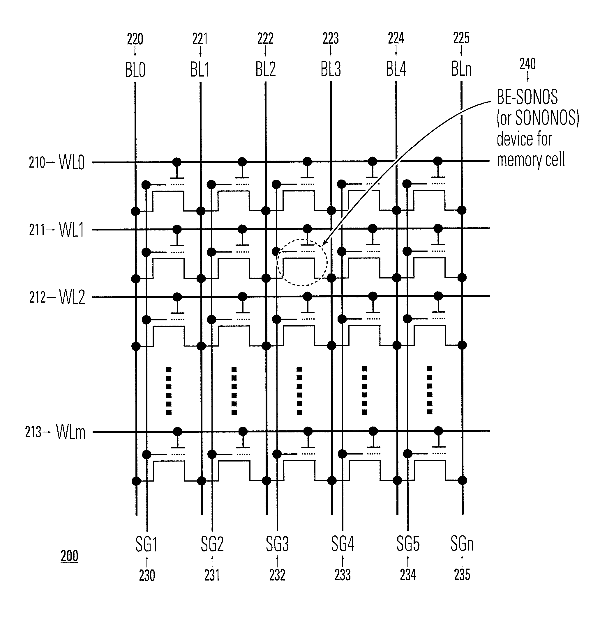
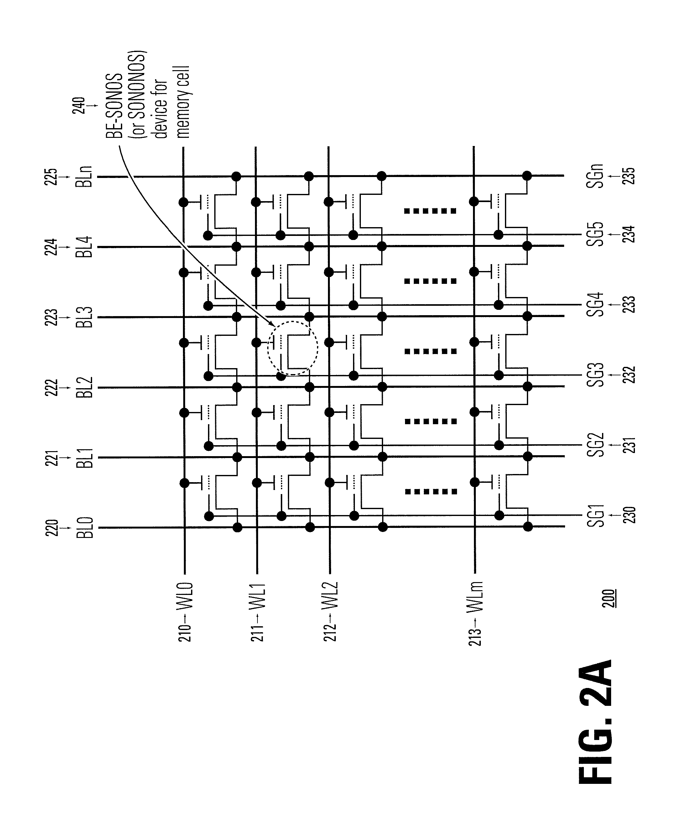
[0045]In FIG. 2A, there is shown a circuit diagram illustrating a BE-SONOS SG-AND array architecture 200 with diffusion bitlines. A plurality of SONONOS devices are connected in parallel to form the BE-SONOS SG-AND array architecture 200. The BE-SONOS array architecture 200 comprises a plurality of wordlines WL0210, WL1211, WL2212, WLm 213 intersecting a plurality of bitlines BL0220, BL1221, BL2222, BL3223, BL4224 and BLn 225. A corresponding sub-gate line is parallel and located nearby a bitline. A sub-gate SG1230 is located adjacent to the bitline BL0220. A sub-gate SG2231 is located adjacent to the bitline BL1221. A sub-gate SG3232 is located adjacent to the bitline BL2222. A sub-gate SG4233 is located adjacent to the bitline BL3223. A sub-gate SG5234 is located adjacent to the bitline BL4224. A sub-gate SGn 235 is located adjacent to the bitline BL5225. A sample BE-SONOS (or SONONOS) device 240 that functions as a memory cell is shown in a circled area.

[0046]As shown in FIG. 2B,...

second embodiment

[0064]In FIG. 10A, there is a circuit diagram illustrating an electrical reset of the SONONOS SGIB-AND array architecture 1000 in the During the electrical reset, the wordlines (or gates) WL0810, WL1811, WL2812, and WLm 813 are set to −10 volts, the bitlines BL0820, BL1821, BL2822, BL3823, BL4824 and BL5825 are left floating, the sub-gates SG0830, SG1831, SG2832, SG3833, SG4834, and SGn 835 are set to 0 volt, and P-well 1010 is set to 5 volts. When a sub-gate SG=is equal to zero volt, that means the SG is not turned on so that there is no inversion bitline. In one embodiment, every fourth sub-gates are connected together such that SG0830 is connected to SG4, SG1831 is connected to SG5, and so on.

[0065]Before operations, the memory circuit 1000 is reset by applying Vgb=−15V (or partition the gate voltage into each WL and p-well), which produces a desirable self-converging property, as shown in the graph 1050 in FIG. 10B. Various circles and triangles in the graph 1050 represent diff...


PUM


Abstract

A bandgap engineered SONOS device structure for design with various AND architectures to perform a source side injection programming method. The BE-SONOS device structure comprises a spacer oxide disposed between a control gate overlaying an oxide-nitride-oxide-nitride-oxide stack and a sub-gate overlaying a gate oxide. In a first embodiment, a BE-SONOS sub-gate-AND array architecture is constructed multiple columns of SONONOS devices with sub-gate lines and diffusion bitlines. In a second embodiment, a BE-SONOS sub-gate-inversion-bitline-AND architecture is constructed multiple columns of SONONOS devices with sub-gate inversion bitlines and with no diffusion bitlines.

Description

BACKGROUND OF THE INVENTION[0001]1. Field of the Invention[0002]The present invention relates generally to non-volatile memory devices, and more particularly, to nitride-based trapping-storage flash memories.[0003]2. Description of Related Art[0004]Electrically programmable and erasable non-volatile memory technologies based on charge storage structures known as Electrically Erasable Programmable Read-Only Memory (EEPROM) and flash memory are used in a variety of modem applications. A flash memory is designed with an array of memory cells that can be independently programmed and read. Sense amplifiers in a flash memory are used to determine the data value or values stored in a non-volatile memory. In a typical sensing scheme, an electrical current through the memory cell being sensed is compared to a reference current by a current sense amplifier.[0005]A number of memory cell structures are used for EEPROM and flash memory. As the dimensions of integrated circuits shrink, greater in...

Claims


Application Information

Patent Timeline
Patent Type & Authority Patents(United States)
IPC IPC(8): G11C11/34G11C16/06
CPCG11C16/0466G11C16/0491H01L29/792H01L27/115H01L27/11568H01L21/28282H01L29/40117H10B43/30H10B69/00H01L29/66833
Inventor LUE, HANG-TINGLIEN, HAO MING
Owner MACRONIX INT CO LTD
Why Eureka
Try Eureka