Using dedicated read output path to reduce unregistered read access time for FPGA embedded memory

a read output path and embedded memory technology, applied in logic circuits, digital storage, instruments, etc., can solve the problems of inability to accept extra time delay introduced by width decoding logic, and introduce substantial time delay, so as to improve memory access speed, improve memory performance, and improve memory access speed

Active Publication Date: 2008-08-19
TAHOE RES LTD
View PDF3 Cites 9 Cited by
  • Summary
  • Abstract
  • Description
  • Claims
  • Application Information

AI Technical Summary

Benefits of technology

[0006]In an embodiment of an invention, a memory unit includes width decoding logic enabling data to be accessed in a memory array using a variety of different data widths. To improve memory access speed, an embodiment of the invention includes a set of dedicated read output paths for accessing data at the full data width of the memory array. The set of dedicated read output paths bypass the width decoding logic and provide data from the memory array directly to a data bus. The read bypass paths provide improved memory performance when width decoding is not needed. Embodiments of the memory unit can be incorporated in programmable devices. The use of the set of read bypass paths or the width decoding logic can be specified with a programmable device configuration. In a further embodiment, hardware applications that require width decoding and improved memory access speed can utilize additional programmable device resources outside the memory unit to register the full width data from the memory unit and convert it to a different data width.

Problems solved by technology

Often, the width decoding logic introduces a substantial time delay due to its large fan-out and capacitive loading.
For user designs requiring high speed memory access, the extra time delay introduced by the width decoding logic can be unacceptable.

Method used


Image

  • Using dedicated read output path to reduce unregistered read access time for FPGA embedded memory
  • Using dedicated read output path to reduce unregistered read access time for FPGA embedded memory
  • Using dedicated read output path to reduce unregistered read access time for FPGA embedded memory

Examples


Embodiment Construction

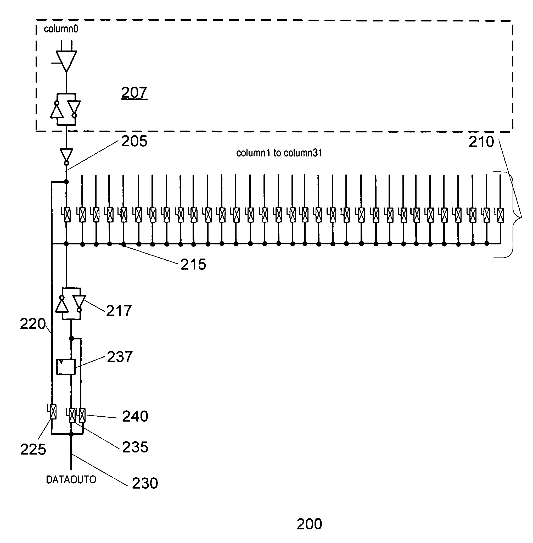
[0014]FIG. 1 illustrates an example prior memory unit 100 of a programmable device. In this example, memory unit 100 has a capacity of 4096 bits of storage, which can be addressed and accessed in widths of 1, 2, 4, 8, 16, and 32 bit at a time. Memory unit 100 includes input path 105. Input path 105 includes input registers for temporarily storing data from other portions of the programmable devices that is to be stored in the memory unit 100. Input path can also include address and control registers for receiving and storing memory addresses and memory unit control and configuration information. Input path 105 can also include control logic for operating the memory unit.

[0015]Write column address decoder 110 decodes the memory addresses associated with incoming data to determine the appropriate column of the memory cell array 125 to store the data. Similarly, row address decoders 112 decodes the memory addresses associated with incoming data to determine the appropriate row of the m...


PUM


Abstract

A memory unit includes width decoding logic enabling data to be accessed in a memory array at different data widths. To improve memory access speed, the memory unit also includes dedicated read output paths for accessing data at the full data width of the memory array. The dedicated read output paths bypass the width decoding logic and provide data from the memory array directly to a data bus, thereby providing improved memory performance when width decoding is not needed. The memory unit can be incorporated in programmable devices and a programmable device configuration can select either the read bypass paths or the width decoding logic. Hardware applications that require width decoding and improved memory access speed can utilize additional programmable device resources outside the memory unit to register the full width data from the memory unit and convert it to a different data width.

Description

BACKGROUND OF THE INVENTION[0001]The invention relates to the field of programmable devices and to memory units adapted to be used within programmable devices. Programmable devices, such as FPGAs, typically include thousands of programmable logic cells that use combinations of logic gates and / or look-up tables to perform logic operations. Programmable devices also include a number of functional blocks having specialized logic devices adapted to specific logic operations, such as adders, multiply and accumulate circuits, phase-locked loops, and one or more memory units for storage and retrieval of data used by the logic cells. The logic cells and functional blocks are interconnected with a configurable switching circuit. The configurable switching circuit selectively routes connections between the logic cells and functional blocks. By configuring the combination of logic cells, functional blocks, and the switching circuit, a programmable device can be adapted to perform virtually any...

Claims


Application Information

Patent Timeline
Patent Type & Authority Patents(United States)
IPC IPC(8): G11C8/02
CPCG11C7/1051G11C7/1057H03K19/1776H03K19/17744G11C7/106G11C2207/105
Inventor YU, HAIMINGKOAY, WEI YEE
Owner TAHOE RES LTD
Why Eureka
Try Eureka