Semiconductor device and method for fabricating the same

a semiconductor device and semiconductor technology, applied in the direction of semiconductor devices, electrical appliances, transistors, etc., can solve the problems of unnecessarily increasing the overall step height reducing the active region (ar) of the semiconductor device, etc., and achieves a high device integration and small size

Inactive Publication Date: 2008-08-26
DONGBU ELECTRONICS CO LTD
View PDF11 Cites 11 Cited by
  • Summary
  • Abstract
  • Description
  • Claims
  • Application Information

AI Technical Summary

Benefits of technology

[0012]An object of the present invention is to provide a semiconductor device in which a storage dielectric film and a storage electrode included in the capacitor is transferred from an active region of a semiconductor substrate to the inactive region thereof, i.e., into a device isolating trench such that the capacitor is prevented from unnecessarily occupying an active region of a semiconductor substrate while maintaining its proper function and a method for fabricating the same.
[0013]Another object of the present invention is to provide a capacitor that is able to maintain a trench structure without having to address the removal of a step height difference, and the active region is minimized in size. Therefore, without having a problem of a step height increase, a finished semiconductor device is able support to high device integration.

Problems solved by technology

Therefore, it becomes more difficult to reduce the active region (AR) of the semiconductor device in accordance with the related art.
However, as recognized by the present inventor in this case, a serious problem additionally occurs that an overall step height of the semiconductor device is unnecessarily increased as much as a height of the stacked capacitor 20.

Method used


Image

  • Semiconductor device and method for fabricating the same
  • Semiconductor device and method for fabricating the same
  • Semiconductor device and method for fabricating the same

Examples


Embodiment Construction

[0023]Reference will now be made in detail to the preferred embodiments of the present invention, examples of which are illustrated in the accompanying drawings. Wherever possible, the same reference numbers will be used throughout the drawings to refer to the same or like parts.

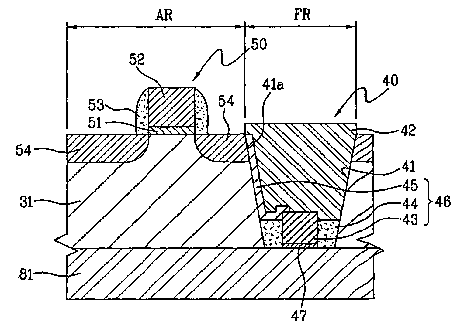
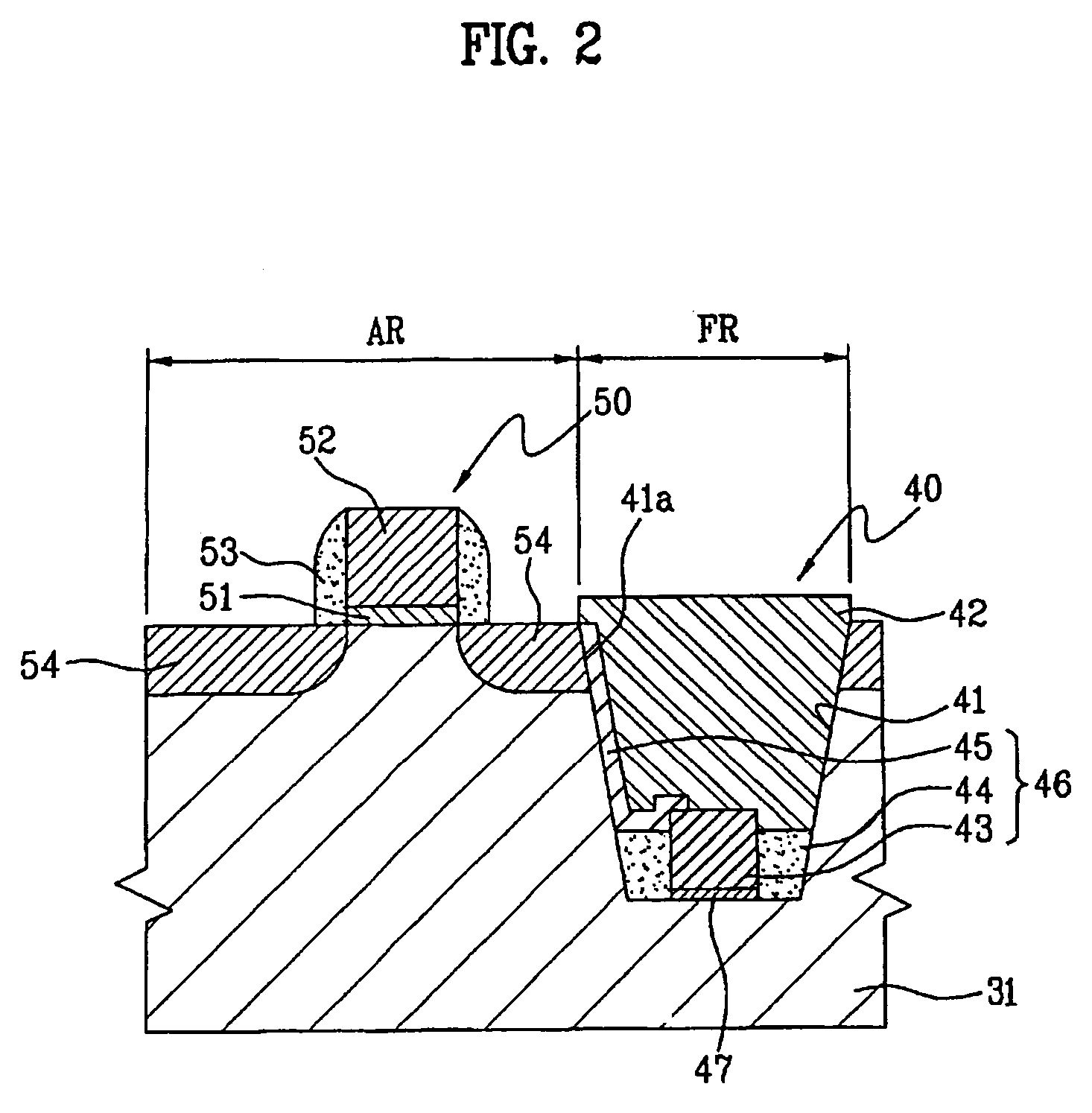
[0024]Hereinafter, referring to the appended drawings, a semiconductor device and a method for fabricating the same will be described in more detail. As illustrated in FIG. 2, in the structure of the semiconductor device in accordance with the present invention, a semiconductor substrate 31 is divided and defined as an inactive region (FR) and an active region (AR) by a device separator 40. In this case, in the active region (AR) of the semiconductor substrate 31, a transistor 50 is disposed for selectively switching a flow of an electric charge to and from a capacitor 46, which holds a charge corresponding to a “1” or a “0”. The transistor 50 includes a gate insulating film pattern 51, a gate electrode patt...


PUM


Abstract

A method creates semiconductor device in which a storage dielectric film and a storage electrode included in the capacitor is transferred from an inactive region of a semiconductor substrate to the active region thereof, i.e., into a device isolating trench such that the capacitor is prevented from unnecessarily occupying an active region of a semiconductor substrate while maintaining its proper function. In contrast to a conventional device where a capacitor is formed in the active region of the semiconductor substrate, to the capacitor is formed in the inactive region according to this process. Accordingly, the capacitor is able to maintain a trench structure without needing to perform a step of removal of a step height difference, and the active region is minimized in size. Therefore, without having a problem of a step height increase, a finished semiconductor device is able to accommodate modern demands for increased device interpretation.

Description

BACKGROUND OF THE INVENTION[0001]1. Field of the Invention[0002]The present invention relates to a semiconductor device and a method for fabricating the same, and more particularly, to a semiconductor device in which a storage dielectric film and a storage electrode included in the capacitor is transferred from an inactive region of a semiconductor substrate to the active region thereof, i.e., into a device isolating trench such that the capacitor is prevented from unnecessarily occupying an active region of a semiconductor substrate while maintaining its proper function, and a method for fabricating the same.[0003]2. Discussion of the Related Art[0004]Recently, the level of integration of a semiconductor device has rapidly progressed, a geometrical structure of each structural element of the semiconductor device has also been greatly reduced.[0005]As illustrated in FIG. 1, in a semiconductor device in accordance with a related art, a semiconductor substrate 1 is divided and defined...

Claims


Application Information

Patent Timeline
Patent Type & Authority Patents(United States)
IPC IPC(8): H01L21/8242H01L21/20H01L21/334H01L21/8234H01L21/8238H01L21/84H01L27/108H01L27/12H01L29/94
CPCH01L21/84H01L27/10829H01L27/1087H01L29/945H01L27/1203H01L29/66181H01L27/10897H10B12/37H10B12/0387H10B12/50H10B99/00
Inventor KOH, KWAN JOO
Owner DONGBU ELECTRONICS CO LTD
Why Eureka
Try Eureka